Publications
2025
299. MXenoids: Generalization of MXene-Inspired Covalent Surface Modifications Across Two-Dimensional Materials
Chenkun Zhou, Young-Hwan Kim, Benjamin Atterberry, Vikash Khokhar, Arashdeep S. Thind, Francisco Lagunas, Ruiming Lin, Di Wang, Wooje Cho, Zirui Zhou, Maia E. Czaikowski, Alexander S. Filatov, John S. Anderson, Robert F. Klie, Richard D. Schaller, De-en Jiang, Aaron J. Rossini, and Dmitri V. Talapin. Journal of the American Chemical Society 2025 Article ASAP.
Abstract
The ability to perform versatile covalent surface modifications in two-dimensional (2D) inorganic materials marks a significant advance in the functionalization of this broad family of materials. One particularly successful example of 2D materials with chemically modifiable surfaces are 2D transition metal carbides and nitrides (MXenes). MXenes’ strong in-plane metal–carbon bonds and labile surface metal–halide bonds create altogether unprecedented opportunities for versatile postsynthetic modifications and assembling complex materials, including various organic–inorganic hybrids. We demonstrate the general applicability of this surface modification strategy to non-MXene halide-terminated 2D materials, termed MXenoids. These surface modifications enable compositional and electronic structure engineering, introduce chiral hybrid organic–inorganic structures, and photoluminescence ranging from near-IR to blue. This study highlights the avenue of surface chemistry-driven materials design, enhancing the functional capabilities of 2D materials.

298. Design of Zn Chalcogenide Shells for Emissive Ga-Rich In1–XGaXAs Quantum Dots Synthesized in Molten Salts
Jun Hyuk Chang, Justin C. Ondry, Danial Zangeneh, Zirui Zhou, Aritrajit Gupta, Yuan Liu, Robert F. Klie, Richard D. Schaller, and Dmitri V. Talapin. ACS Nano 2025 Article ASAP.
Abstract
Colloidal quantum dots (QDs) have seen expanded applications in optoelectronics from visible to near-infrared (NIR) wavelengths. However, the options for QDs with bright and size-tunable emission in the NIR region are mostly limited to heavy-metal-based (Pb, Cd, Hg) semiconductors. Here, Ga-rich In1–XGaXAs QDs with zinc chalcogenide shells are demonstrated as candidates for NIR emitters. Based on new developments in inorganic molten salt chemistry, we synthesized colloidal In1–XGaXAs QDs containing up to 85% gallium with high crystallinity based on Raman and XRD analyses. Zinc selenide and sulfide shells with different morphologies were grown on In1–XGaXAs QDs by controlling the Zn precursor chemistry. Despite the nominally reduced lattice mismatch in the In1–XGaXAs/ZnSe heterostructure, a ZnS shell was found to be a much more effective passivation material: In1–XGaXAs/ZnS core–shell QDs show a photoluminescence quantum yield (PL QY) of about 30% versus 11% for ZnSe shells. Based on the analysis of PL decay and transient absorption (TA) dynamics, we surmise that electron trapping is the major reason for efficiency loss, providing a clear heterostructure design principle for realizing efficient NIR-emitting In1–XGaXAs QDs.

297. In Situ Raman and Fourier Transform Infrared Spectroscopy Studies of MXene−Electrolyte Interfaces
Tetiana Parker, Yuan Zhang, Kateryna Shevchuk, Teng Zhang, Vikash Khokhar, Young-Hwan Kim, Givi Kadagishvili, David Bugallo, Manushree Tanwar, Ben Davis, Jongyoun Kim, Zahra Fakhraai, Yong-Jie Hu, De-en Jiang, Dmitri V. Talapin, and Yury Gogotsi. ACS Nano 2025 2025, 19, 24, 22228–22239
Abstract
A comprehensive understanding of electrochemical interfaces is essential for the optimal performance of electrocatalysts, supercapacitors, and batteries. However, understanding the electrochemical behavior of MXenes during electrochemical processes by any single technique does not provide a whole picture. We achieved real-time monitoring in the complete near-mid-infrared chemical range by utilizing Raman spectroscopy (near-infrared (NIR) excitation) and Fourier transform infrared (FTIR) spectroscopy in the mid-infrared (MIR) range. The change of intramolecular O−H vibrations of MXene-confined water was monitored in real time using FTIR, while surface terminations were monitored by using Raman spectroscopy. The dynamic interplay between charge storage and the change in MXene surface chemistry was studied by employing representative electrolytes (0.5 M H2SO4, 1 M LiCl, and 6 M KOH) and comparing hydrophilic Ti3C2Tx with mixed-terminations (T = O/OH/F) with hydrophobic chlorine-terminated Ti3C2Cl2 MXene electrodes. Ab initio molecular dynamics (MD) simulations and density functional theory (DFT) calculations were used to shed light on ion insertion with a dynamic change of ion solvation and reveal the structure of the MXene-confined water.

296. Engineering spin coherence in core-shell diamond nanocrystals
Uri Zvi, Denis R. Candido, Adam M. Weiss, Aidan R. Jones, Lingjie Chen, Iryna Golovina, Xiaofei Yu, Stella Wang, Dmitri V. Talapin, Michael E. Flatté, Aaron P. Esser-Kahn, and Peter C. Maurer. Proceedings of the National Academy of Sciences 2025 122, 21, e2422542122
Abstract
Fluorescent diamond nanocrystals can host spin qubit sensors capable of probing the physical properties of biological systems with nanoscale spatial resolution. Sub-100 nm diamond nanosensors can readily be delivered into intact cells and even living organisms. However, applications beyond current proof-of-principle experiments require a substantial increase in sensitivity, which is limited by surface induced charge instability and electron-spin dephasing. In this work, we utilize engineered core-shell structures to achieve a drastic increase in qubit coherence times (T2) from 1.1 to 35 μs in bare nanodiamonds to upward of 52 to 87 μs. We use electron-paramagnetic-resonance results to present a band bending model and connect silica encapsulation to the removal of deleterious mid-gap surface states that are negatively affecting the qubit’s spin properties. Combined with a 1.9-fold increase in particle luminescence these advances correspond to up to two-order-of-magnitude reduction in integration time. Probing qubit dynamics at a single particle level further reveals that the noise characteristics fundamentally change from a bath with spins that rearrange their spatial configuration during the course of an experiment to a more dilute static bath. The observed results shed light on the underlying mechanisms governing fluorescence and spin properties in diamond nanocrystals and offer an effective noise mitigation strategy based on engineered core-shell structures.

295. Exciton-phonon coupling and phonon-assisted exciton relaxation dynamics in In1-xGaxP quantum dots
Beiye C. Li, Kailai Lin, Ping-Jui E. Wu, Aritrajit Gupta, Kaiyue Peng, Siddhartha Sohoni, Justin C. Ondry, Zirui Zhou, Caitlin C. Bellora, Young Jay Ryu, Stella Chariton, David J. Gosztola, Vitali B. Prakapenka, Richard D. Schaller, Dmitri V. Talapin, Eran Rabani and Gregory S. Engel. Nature Communications 2025 16, 4424
Abstract
Quantum dots leverage quantum confinement to modify the electronic structure of materials, separating electronic transitions from the composition of the corresponding bulk material. With ternary quantum dots, the composition may be varied continuously so that both composition and size may be used to tune the bandgap. As composition influences electron-phonon coupling which in turn governs relaxation dynamics, the composition of ternary quantum dots may be adjusted to change dynamics. Here, we show that exciton-phonon coupling and phonon-assisted exciton relaxation dynamics remain strongly correlated to material composition in ternary In0.62Ga0.38P/ZnS and In0.35Ga0.65P/ZnS quantum dots using both experimental two-dimensional electronic spectroscopy measurements and quantum dynamical simulations. Theoretical calculations show that alloyed In1-xGaxP quantum dots have more complex exciton level structure than parent InP quantum dots. We identify a slower hot exciton cooling rate in In0.62Ga0.38P/ZnS, attributed to the presence of ‘energy-retaining’ valley exciton states with strong exciton-phonon coupling. Experimental quantum beating maps reveal a more localized quantum beat pattern for In0.35Ga0.65P/ZnS quantum dots, which may relate to the increased number of ‘dim’ exciton levels with reduced spacings. These findings highlight that exciton relaxation dynamics and exciton-phonon coupling in an alloyed In1-xGaxP quantum dot system are composition-dependent.

294. Ultrafast Dynamics of Plasmon-Coupled Excitons in Semiconducting Nanoplatelets
Wei Wang, Daniel Rosenmann, Yuzi Liu, Xuedan Ma, Wooje Cho, Joshua Portner, Ruiming Lin, Dmitri V. Talapin, Ralu Divan, David J. Gosztola, Stephen K. Gray, and Gary P. Wiederrecht. Journal of Physical Chemistry C 2025 129, 16, 7804-7812
Abstract
Exciton-plasmon coupling in nanomaterials produces many relevant phenomena for photonics applications including increased light-matter interactions, enhanced radiative rates of quantum emitters, and coherent energy exchange. In the case of exciton coupling to surface plasmon polaritons (SPPs), dispersive interactions controlled by the wavevector of optical excitation create the opportunity for tunable optical emission. Strong temporal impacts on exciton lifetimes can also occur in coupled systems, creating the opportunity for ultrafast control of exciton lifetime via changes in electronic coupling magnitude to a dispersive SPP. The coupling strength can be impacted by the morphology of the nanomaterials. Here, we utilize colloidal semiconductor nanoplatelets deposited onto thin silver plasmonic films, and compare the results to semiconductor quantum dots deposited on the silver films. We map the dispersion of the coupled systems and measure the ultrafast transient absorption response of the coupled systems. Due to the larger interaction areas of the nanoplatelets that lie flat on the silver films, a greater degree of coupling is found for the nanoplatelets, and much faster temporal responses are found as compared to quantum dots. Fresnel theory calculations that incorporate heavy and light hole features can reproduce the dispersion of the nanoplatelet-silver film, and a simple three-state model is developed to provide insights into the nature of the coupling at different photon energies along the dispersion curve.

293. Ligand-Engineered Direct Optical Lithography of Nanocrystals with Industrially Compatible Solvents
Pengwei Xiao, Jianhang Ma, Zhoufan Zhang, Yihao Zou, Huanhuan Luo, Jie Guan, Jian-rong Zhang, Likuan Zhou, Wenjun Hou, Panke Zhang, Dmitri V. Talapin, and Yuanyuan Wang. ACS Nano 2025, 19, 14, 14509–14520
Abstract
Nondestructive and precise patterning of colloidal semiconductor nanocrystals (NCs) is critical in the fabrication of solution-processable optoelectronic devices. Direct optical lithography of functional inorganic nanomaterials (DOLFIN) is widely used for the high-resolution patterning of NCs. However, conventional DOLFIN chemistry relies on solvents incompatible with mainstream industrial lithography processes, which impedes DOLFN’s widespread adoption as a universal technology for real-world additive manufacturing. In this work, we proposed specific criteria for ligand design and designed a series of multifunctional ligands combining methacrylate and carboxyl groups. Such ligands allowed us to colloidally stabilize and optically pattern NCs with i-line and h-line light sources by using industrially friendly solvents. We showed that single-color and multicolor patterns with a spatial resolution of 1 μm can be achieved without compromising the optical and optoelectronic properties. The patterned NC films showed photoluminescence (PL) and electroluminescence (EL) on par with those of unpatterned films. The red-emitting QLEDs showed a peak external quantum efficiency (EQE) of 22.0%. The ability to reliably pattern bright NCs from PGMEA will facilitate the adoption of DOLFIN as an industrialized system-level integration platform and will significantly impact the production of high-resolution, full-color QLED devices.

292. Colloidal Chemistry in Molten Inorganic Salts: Direct Synthesis of III–V Quantum Dots via Dehalosilylation of (Me3Si)3Pn (Pn = P, As) with Group III Halides
Zirui Zhou, Justin C. Ondry, Yi-Chun Liu, Haoqi Wu, Ahhyun Jeong, Aritrajit Gupta, Yi-Chen Chen, Jun Hyuk Chang, Richard D. Schaller, and Dmitri V. Talapin. Journal of the American Chemical Society 2025, 147, 11, 9198–9209
Abstract
Gallium pnictides, such as GaAs and GaP, are among the most widely used semiconductors for electronic, optoelectronic, and photonic applications. However, solution syntheses of gallium pnictide nanomaterials are less developed than those of many other colloidal semiconductors, including indium pnictides, II–VI and IV–VI compounds, and lead halide perovskites. In this work, we demonstrate that the Wells dehalosilylation reaction can be carried out in molten inorganic salt solvents to synthesize colloidal GaAs, GaP, and GaP1–xAsx nanocrystals. We demonstrate that discrete colloidal nanocrystals can be nucleated and grown in a molten salt with control over their size and composition. Additionally, we found that reaction temperatures above 400 °C are crucial for annealing structural defects in GaAs nanocrystals. We also highlight the utility of the as-synthesized GaP nanocrystals by showing that GaP can be solution-processed into high-refractive-index coatings and patterned by direct optical lithography with micron resolution. Finally, we demonstrate that dehalosilylation reactions in molten salts can be generalized to synthesize indium pnictide (Pn = As, P) and ternary (In1–xGaxAs and In1–xGaxP) quantum dots.

291. Bound and Continuum Intersubband Transitions in Colloidal Quantum Wells
Benjamin T. Diroll, Igor Coropceanu, Joshua Portner, Muchuan Hua, Richard D. Schaller, and Dmitri V. Talapin. Nano Letters 2025 25, 6, 2366–2372
Abstract
Quantum well intersubband transitions are critical for quantum cascade lasers and infrared photodetectors. Control of band offsets allows bound-to-bound intersubband transitions, with confinement of both initial and final states, and bound-to-continuum transitions, in which only the initial state is energetically confined within the potential well. Both types of transitions are also achieved in colloidal CdSe wells by changing the heterostructure shell. Bare wells have narrow intersubband transitions spanning the near-infrared spectrum following effective mass predictions. Atomically precise core/shells enable a readily adjusted potential well for electrons. For CdSe/ZnS, bound-to-bound transitions are narrow and redshift with shell thickness. By contrast, broad bound-to-continuum absorptions are found in CdSe/CdS. Due to small conduction band offsets, higher conduction band states of the well are more delocalized into the CdS shell. These measurements provide unique data to understand the electronic structure of colloidal quantum wells and chart a path to atomically precise optoelectronic materials for the mid-infrared.

290. In Situ Formation of Ripplocations in Hybrid Organic–Inorganic MXenes
Francisco Lagunas, Chenkun Zhou, Di Wang, Anupma Thakur, Babak Anasori, Dmitri V. Talapin, Zachary D. Hood, and Robert F. Klie. Advanced Materials 2025 37, 13, 2411669
Abstract
Inorganic–organic hybrid MXenes (h-MXenes) are a family of 2D transition metal carbides and nitrides functionalized with alkylimido and alkylamido surface groups. Using cryogenic and room temperature scanning transmission electron microscopy (STEM) and electron energy-loss spectroscopy (EELS), it is shown that ripplocations, a form of a fundamental defect in 2D and layered structures, are abundant in this family of materials. Furthermore, detailed studies of electron probe sample interactions, focusing on structural deformations caused by the electron beam are presented. The findings indicate that at cryogenic temperatures (≈100 K) and below a specific dose threshold, the structure of h-MXenes remains largely intact. However, exceeding this threshold leads to electron beam-induced deformation through ripplocations. Interestingly, the deformation behavior, required dose, and resultant structure are highly dependent on temperature. At 100 K, it is demonstrated that the electron beam can induce ripplocations in situ with a high degree of precision.

2024
289. Ultrafast Symmetry Control in Photoexcited Quantum Dots
Burak Guzelturk, Joshua Portner, Justin Ondry, Samira Ghanbarzadeh, Mia Tarantola, Ahhyun Jeong, Thomas Field, Alicia M. Chandler, Eliza Wieman, Thomas R. Hopper, Nicolas E. Watkins, Jin Yu, Xinxin Cheng, Ming-Fu Lin, Duan Luo, Patrick L. Kramer, Xiaozhe Shen, Alexander H. Reid, Olaf Borkiewicz, Uta Ruett, Xiaoyi Zhang, Aaron M. Lindenberg, Jihong Ma, Richard D. Schaller, Dmitri V. Talapin, and Benjamin L. Cotts. Advanced Materials 2024 37, 4, 2414196
Abstract
Symmetry control is essential for realizing unconventional properties, such as ferroelectricity, nonlinear optical responses, and complex topological order, thus it holds promise for the design of emerging quantum and photonic systems. Nevertheless, fast and reversible control of symmetry in materials remains a challenge, especially for nanoscale systems. Here, reversible symmetry changes are unveiled in colloidal lead chalcogenide quantum dots on picosecond timescales. Using a combination of ultrafast electron diffraction and total X-ray scattering, in conjunction with atomic-scale structural modeling and first-principles calculations, it is revealed that symmetry-broken lead sulfide quantum dots restore to a centrosymmetric phase upon photoexcitation. The symmetry restoration is driven by photoexcited electronic carriers, which suppress lead off-centering for about 100 ps. Furthermore, the change in symmetry is closely correlated with the electronic properties, and the bandgap transiently red-shifts in the symmetry-restored quantum dots. Overall, this study elucidates reversible symmetry changes in colloidal quantum dots, and more broadly defines a new methodology to optically control symmetry in nanoscale systems on ultrafast timescales.

288. Colloidal Dispersions of Sterically and Electrostatically Stabilized PbS Quantum Dots: Structure Factors, Second Virial Coefficients, and Film-Forming Properties
Ahhyun Jeong, Joshua Portner, Christian P. N. Tanner, Justin C. Ondry, Chenkun Zhou, Zehan Mi, Youssef A. Tazoui, Byeongdu Lee, Vivian R. K. Wall, Naomi S. Ginsberg, and Dmitri V. Talapin. ACS Nano 2024 18, 50, 33864–33874
Abstract
Electrostatically stabilized nanocrystals (NCs) and, in particular, quantum dots (QDs) hold promise for forming strongly coupled superlattices due to their compact and electronically conductive surface ligands. However, studies of the colloidal dispersion and interparticle interactions of electrostatically stabilized sub-10 nm NCs have been limited, hindering the optimization of their colloidal stability and self-assembly. In this study, we employed small-angle X-ray scattering (SAXS) experiments to investigate the interparticle interactions and arrangement of PbS QDs with thiostannate ligands (PbS–Sn2S64–) in polar solvents. The study reveals significant deviations from the ideal solution behavior in electrostatically stabilized QD dispersions. Our results demonstrate that PbS–Sn2S64– QDs exhibit long-range interactions within the solvent, in contrast to the short-range steric repulsion characteristic of PbS QDs with oleate ligands (PbS-OA). Introducing highly charged multivalent electrolytes screens electrostatic interactions between charged QDs, reducing the length scale of the repulsive interactions. Furthermore, we calculated the second virial (B2) coefficients from SAXS data, providing insights into how surface chemistry, solvent, and size influence pair potentials. Finally, we explore the influence of long-range interparticle interactions of PbS–Sn2S64– QDs on the morphology of films produced by drying or spin-coating colloidal solutions. The long-range repulsive term of PbS–Sn2S64– QDs promotes the formation of amorphous films, and screening the electrostatic repulsion by the addition of an electrolyte enables the formation of crystalline domains. These findings highlight the critical role of NC–NC interactions in tailoring the properties of functional materials made of colloidal NCs.

287. Reductive pathways in molten inorganic salts enable colloidal synthesis of III-V semiconductor nanocrystals
Justin C. Ondry, Zirui Zhou, Kailai Lin, Aritrajit Gupta, Jun Hyuk Chang, Haoqi Wu, Ahhyun Jeong, Benjamin F. Hammel, Di Wang, H. Christopher Fry, Sadegh Yazdi, Gordana Dukovic, Richard D. Schaller, Eran Rabani, and Dmitri V. Talapin. Science 2024 386, 6720, 401-407
Abstract
Colloidal quantum dots, with their size-tunable optoelectronic properties and scalable synthesis, enable applications in which inexpensive high-performance semiconductors are needed. Synthesis science breakthroughs have been key to the realization of quantum dot technologies, but important group III–group V semiconductors, including colloidal gallium arsenide (GaAs), still cannot be synthesized with existing approaches. The high-temperature molten salt colloidal synthesis introduced in this work enables the preparation of previously intractable colloidal materials. We directly nucleated and grew colloidal quantum dots in molten inorganic salts by harnessing molten salt redox chemistry and using surfactant additives for nanocrystal shape control. Synthesis temperatures above 425°C are critical for realizing photoluminescent GaAs quantum dots, which emphasizes the importance of high temperatures enabled by molten salt solvents. We generalize the methodology and demonstrate nearly a dozen III-V solid-solution nanocrystal compositions that have not been previously reported.
Read this paper for free here!

286. Evolution of Surface Chemistry in Two-Dimensional MXenes: From Mixed to Tunable Uniform Terminations
Mengni Jiang, Di Wang, Young-Hwan Kim, Chunying Duan, Dmitri V. Talapin, and Chenkun Zhou. Angewandte Chemie International Edition 2024 63, 37, e202409480
Abstract

285. In situ coherent x-ray scattering reveals polycrystalline structure and discrete annealing events in strongly coupled nanocrystal superlattices
Matthew J. Hurley, Christian P. N. Tanner, Joshua Portner, James K. Utterback, Igor Coropceanu, Avishek Das, Joseph D. Slivka, Andrei Fluerasu, Yanwen Sun, Sanghoon Song, Leo M. Hamerlynck, Alexander H. Miller, Priyadarshini Bhattacharyya, Dmitri V. Talapin, Garth J. Williams, Naomi S. Ginsberg, and Samuel W. Teitelbaum. Physical Review Research 2024 6, 023119
Abstract

284. Spectrally engineered textile for radiative cooling against urban heat islands
Ronghui Wu, Chenxi Sui, Ting-Hsuan Chen, Zirui Zhou, Qizhang Li, Gangbin Yan, Yu Han, Jiawei Liang, Pei-Jan Hung, Edward Luo, Dmitri V. Talapin, and Po-Chun Hsu. Science 2024 384, 6701, 1203-1212
Abstract
Radiative cooling textiles are promising for achieving personal thermal comfort under the increasing global temperature. However, urban areas have heat island effects that largely diminish the effectiveness of cooling textiles as wearable fabrics because they absorb emitted radiation from the ground and nearby buildings. We developed a mid-infrared (MIR) spectrally selective hierarchical fabric (SSHF) with emissivity greatly dominant in the atmospheric transmission window (ATW) through molecular design, minimizing the net heat gain from the surroundings. The SSHF features a high solar spectrum reflectivity of 0.97 owing to the strong Mie scattering from the nano-micro hybrid fibrous structure. SSHF is 2.3°C cooler than a solar-reflecting broadband emitter when placed vertically in simulated outdoor urban scenarios during the day while also having excellent wearable properties.

283. Nanocrystal Assemblies: Current Advances and Open Problems
Carlos L. Bassani, Greg van Anders, Uri Banin, Dmitry Baranov, Qian Chen, Marjolein Dijkstra, Michael S. Dimitriyev, Efi Efrati, Jordi Faraudo, Oleg Gang, Nicola Gaston, Ramin Golestanian, G. Ivan Guerrero-Garcia, Michael Gruenwald, Amir Haji-Akbari, Maria Ibáñez, Matthias Karg, Tobias Kraus, Byeongdu Lee, Reid C. Van Lehn, Robert J. Macfarlane, Bortolo M. Mognetti, Arash Nikoubashman, Saeed Osat, Oleg V. Prezhdo, Grant M. Rotskoff, Leonor Saiz, An-Chang Shi, Sara Skrabalak, Ivan I. Smalyukh, Mario Tagliazucchi, Dmitri V. Talapin, Alexei V. Tkachenko, Sergei Tretiak, David Vaknin, Asaph Widmer-Cooper, Gerard C. L. Wong, Xingchen Ye, Shan Zhou, Eran Rabani, Michael Engel, and Alex Travesset. ACS Nano 2024 18, 23, 14791-14840
Abstract
We explore the potential of nanocrystals (a term used equivalently to nanoparticles) as building blocks for nanomaterials, and the current advances and open challenges for fundamental science developments and applications. Nanocrystal assemblies are inherently multiscale, and the generation of revolutionary material properties requires a precise understanding of the relationship between structure and function, the former being determined by classical effects and the latter often by quantum effects. With an emphasis on theory and computation, we discuss challenges that hamper current assembly strategies and to what extent nanocrystal assemblies represent thermodynamic equilibrium or kinetically trapped metastable states. We also examine dynamic effects and optimization of assembly protocols. Finally, we discuss promising material functions and examples of their realization with nanocrystal assemblies.

282. Nanolaser Using Colloidal Quantum Wells Deterministically Integrated on a Nanocavity
David Sharp, Ruiming Lin, Hao Nguyen, Arnab Manna, Hannah Rarick, Christopher Munley, Wooje Cho, Dmitri Talapin, Brandi Cossairt, and Arka Majumdar. ACS Photonics 2024 11, 6, 2465–2470
Abstract
On-chip light sources based on hybrid integration of colloidal semiconductor nanocrystal emitters with integrated photonics have focused on either colloidal emitters ill-suited to act as gain media due to large Auger recombination or nonscalable suspended nanocavity geometries with a randomly positioned colloidal gain material. In this work, we demonstrate a nanolaser by integrating colloidal quantum wells with an on-substrate nanobeam cavity geometry. We employ deterministic positioning of colloidal quantum wells to enhance the coupling of the gain material to the cavity. This device achieves lasing under continuous-wave optical pumping at room temperature with a threshold of 2.9 μW, which demonstrates the suitability of this hybrid platform for scalable on-chip light sources. Additionally, we show that the shelling of the colloidal quantum wells is essential for maximizing gain.

281. In Situ X-ray Scattering Reveals Coarsening Rates of Superlattices Self-Assembled from Electrostatically Stabilized Metal Nanocrystals Depend Nonmonotonically on Driving Force
Christian P. N. Tanner, James K. Utterback, Joshua Portner, Igor Coropceanu, Avishek Das, Christopher J. Tassone, Samuel W. Teitelbaum, David T. Limmer, Dmitri V. Talapin, and Naomi S. Ginsberg. ACS Nano 2024, 18, 7, 5778–5789
Abstract
Self-assembly of colloidal nanocrystals (NCs) into superlattices (SLs) is an appealing strategy to design hierarchically organized materials with promising functionalities. Mechanistic studies are still needed to uncover the design principles for SL self-assembly, but such studies have been difficult to perform due to the fast time and short length scales of NC systems. To address this challenge, we developed an apparatus to directly measure the evolving phases in situ and in real time of an electrostatically stabilized Au NC solution before, during, and after it is quenched to form SLs using small-angle X-ray scattering. By developing a quantitative model, we fit the time-dependent scattering patterns to obtain the phase diagram of the system and the kinetics of the colloidal and SL phases as a function of varying quench conditions. The extracted phase diagram is consistent with particles whose interactions are short in range relative to their diameter. We find the degree of SL order is primarily determined by fast (subsecond) initial nucleation and growth kinetics, while coarsening at later times depends nonmonotonically on the driving force for self-assembly. We validate these results by direct comparison with simulations and use them to suggest dynamic design principles to optimize the crystallinity within a finite time window. The combination of this measurement methodology, quantitative analysis, and simulation should be generalizable to elucidate and better control the microscopic self-assembly pathways of a wide range of bottom-up assembled systems and architectures.

280. Synthesis of Ternary and Quaternary Group III-Arsenide Colloidal Quantum Dots via High-Temperature Cation Exchange in Molten Salts: The Importance of Molten Salt Speciation
Justin C. Ondry, Aritrajit Gupta, Zirui Zhou, Jun Hyuk Chang, and Dmitri V. Talapin. ACS Nano 2024, 18, 1, 858–873
Abstract
Colloidal semiconductor nanocrystals are an important class of materials which have many desirable optoelectronic properties. In their bulk phases, gallium- and aluminum-containing III–V materials such as GaAs, GaP, and Al1–xGaxAs represent some of the most technologically important semiconductors. However, their colloidal synthesis by traditional methods is difficult due to the high temperatures needed to crystallize these highly covalent materials and the extreme reactivity of Ga- and Al- precursors toward organic solvents at such high temperatures. A recently developed paradigm shift in the synthesis of these materials is to use molten inorganic salts as solvents to prepare Ga- containing III–V colloidal nanocrystals by cation exchange of the corresponding indium pnictide (InPn) colloidal nanocrystals. There have been several successful applications of molten salt solvents to prepare III-phosphide colloidal nanocrystals. However, little is known about the nature of these reaction environments at the relevant reaction conditions and synthesis of III-arsenide colloidal nanocrystals remains challenging. Herein we report a detailed study on cation exchange of InPn nanocrystals using nominally Lewis basic molten salt solvents with added gallium halides. Surprisingly, these salt systems phase separate into two immiscible phases, and the nanocrystals preferentially segregate to one of the phases. Using a suite of in situ spectroscopy tools, we identify the phase the nanocrystals segregate to as Lewis neutral alkali tetrahalogallate molten salts. We apply in situ high-temperature Raman spectroscopy to identify the chemical species present in several molten salt compositions at experimentally relevant reaction conditions to elucidate a molecular basis for the reactivity observed. We then employ Lewis neutral KGaI4 molten salts to prepare high-quality In1–xGaxAs and In1–xGaxP nanocrystals and demonstrate that deviation from Lewis neutral conditions accelerate nanocrystal decomposition in the case of III-arsenide materials. Further, we expand to KAlI4-based molten salts to prepare In1–x–yGaxAlyAs nanocrystals which represent an example of solution-synthesized quaternary III–V nanocrystals. These insights provide a molecular basis for the rational development of molten salt solvents, thus allowing the preparation of a diverse array of multicomponent III–V colloidal nanocrystals.

2023
279. Direct Optical Lithography of Colloidal InP-based Quantum Dots with Ligand Pair Treatment
Jaehwan Lee, Jaeyeong Ha, Hyunjin Cho, Doh C. Lee, Hyungdoh Lee, Dmitri V. Talapin, and Himchan Cho. ACS Energy Lett. 2023, 8, 10, 4210-4217
Abstract
Direct optical lithography presents a promising patterning method for colloidal quantum dots (QDs). However, additional care needs to be taken to prevent deterioration of the optical properties of QDs upon the patterning process, especially for InP-based QDs. This study proposes an efficient method for high-resolution patterning of InP-based QDs using a photoacid generator, while preserving their optical properties. Specifically, our solid-state ligand exchange strategy, replacing chloride ligands with long-chain amine/carboxylate pair-ligands, successfully recovered the photoluminescence quantum yield (PLQY) of the patterned InP-based QD films to ~67% of the original PLQY. Upon examining the origins of the PLQY reduction during patterning, we concluded that the formation of deep traps caused by the exchanged chloride ligands was the primary cause. Finally, we fabricated high-resolution (feature size: 1 µm), multicolored patterns of InP-based QDs, thereby demonstrating the potential of the proposed patterning method for next-generation high-resolution displays and optoelectronic devices.

278. Designer quantum dot molecules and beyond (News and Views)
James Cassidy, Justin C. Ondry, and Dmitri V. Talapin. Nature Mater. 2023, 22, 1167-1168
Abstract
Quantum dots couple to form artificial molecules that allow for variable colour emission in response to an electric field.
Atoms as the building blocks of matter and the chemical bonds between atoms remain fundamental concepts in chemistry. Covalent and ionic bonds between atoms were elegantly described by Linus Pauling’s notion of electronegativity, which was further developed by Robert Mulliken who introduced the molecular orbital theory. Now, with the advancement of nanoscience, it may become possible to expand and generalize the concepts of ‘atom’ and ‘chemical bond’. Quantum dots (QDs), which are nanometre-sized semiconductor crystals, are sometimes referred to as ‘artificial atoms’ owing to their discrete electronic energy levels that closely resemble electronic states of atoms. The electronic structure of QDs can be continuously varied, something that cannot be done with traditional atoms found in the periodic table. There now exists an opportunity to develop a paradigm that uses QDs with precisely engineered sizes, shapes, compositions and concomitant electronic structures for building ‘artificial molecules’ and ‘artificial solids’. Just as atoms combine to form molecules with properties dramatically different from those of the atomic constituents, electronic bonding of QDs will lead to new structures that can be called colloidal quantum dot molecules (CQDMs). Now, writing in Nature Materials, Ossia et al. report that QDs coupled together into a CQDM can demonstrate optoelectronic signatures of an artificial bond that forms between two colloidal QDS.

277. The Ligand–Surface Interface and Its Influence on Nanoparticle Properties (Guest Editorial)
Jwa-Min Nam, Jonathan S. Owen, and Dmitri V. Talapin. Acc. Chem. Res. 2023, 56, 17, 2265–2266 (Editorial for Special Issue: Ligand and Surface Chemistry of Nanoparticles)
Abstract
Colloidal nanoparticles of semiconductors, metals, magnets, and other functional materials have been actively researched for several decades by both academic and industrial scientists and engineers. Colloidal nanoparticles offer insights into the peculiarities of nucleation and growth and the reactivity of surfaces, while the industry sees in nanoparticles a unique opportunity to combine functionalities typical for inorganic solids with structural flexibility and processability of polymers. Central to both of these pursuits is the interface between the inorganic nanoparticle core and the surface ligands that are covalently or electrostatically bound to the core surface. These surface ligands are integral components of nanomaterials. They direct nanoparticle formation, influence their chemical reactivity and electronic structure, and mediate interactions with the environment. The study of core–ligand interaction and the design of new ways to diversify the ligands is therefore an area of study that is inextricably linked to nanoscience.

276. Stimuli-Responsive Surface Ligands for Direct Lithography of Functional Inorganic Nanomaterials
Jia-Ahn Pan, Himchan Cho, Igor Coropceanu, Haoqi Wu, and Dmitri V. Talapin. Acc. Chem. Res. 2023, 56, 17, 2286–2297
Abstract
Colloidal nanocrystals (NCs) have emerged as a diverse class of materials with tunable composition, size, shape, and surface chemistry. The integration of colloidal nanomaterials in real-world devices is held back by challenges in making patterned NC films with the resolution, throughput, and cost demanded by device components and applications. Therefore, suitable approaches to pattern NCs need to be established to aid the transition from individual proof-of-concept NC devices to integrated and multiplexed technological systems. In this Account, we discuss the development of stimuli-sensitive surface ligands that enable NCs to be patterned directly with good pattern fidelity while retaining desirable properties. We focus on rationally selected ligands that enable changes in the NC dispersibility by responding to light, electron beam, and/or heat. First, we summarize the fundamental forces between colloidal NCs and discuss the principles behind NC stabilization/destabilization. Six ligand-based patterning mechanisms are introduced: ligand cross-linking, ligand decomposition, ligand desorption, in situ ligand exchange, ion/ligand binding, and ligand-aided increase of ionic strength. We then discuss relevant figures-of-merit that should be considered when choosing a particular ligand chemistry or stimulus for patterning NCs. We also give examples of proof-of-concept patterned NC devices and evaluate their performance. Finally, we provide an outlook on further expanding the chemistry of stimuli-sensitive ligands, improving the NC pattern quality, progress toward 3D printing, and other potential research directions. Ultimately, we hope that the development of a patterning toolbox for NCs will expedite their implementation in a broad range of applications

275. Periplasmic biomineralization for semi-artificial photosynthesis
Yiliang Lin, Jiuyun Shi, Wei Feng, Jiping Yue, Yanqi Luo, Si Chen, Bin Yang, Yuanwen Jiang, Huicheng Hu, Chenkun Zhou, Fengyuan Shi, Aleksander Prominski, Dmitri V, Talapin, Wei Xiong, Xiang Gao, and Bozhi Tian. Science Adv. 2023, 9, 29, sciadv.adg5858
Abstract
Semiconductor-based biointerfaces are typically established either on the surface of the plasma membrane or within the cytoplasm. In Gram-negative bacteria, the periplasmic space, characterized by its confinement and the presence of numerous enzymes and peptidoglycans, offers additional opportunities for biomineralization, allowing for nongenetic modulation interfaces. We demonstrate semiconductor nanocluster precipitation containing single- and multiple-metal elements within the periplasm, as observed through various electron- and x-ray-based imaging techniques. The periplasmic semiconductors are metastable and display defect-dominant fluorescent properties. Unexpectedly, the defect-rich (i.e., the low-grade) semiconductor nanoclusters produced in situ can still increase adenosine triphosphate levels and malate production when coupled with photosensitization. We expand the sustainability levels of the biohybrid system to include reducing heavy metals at the primary level, building living bioreactors at the secondary level, and creating semi-artificial photosynthesis at the tertiary level. The biomineralization-enabled periplasmic biohybrids have the potential to serve as defect-tolerant platforms for diverse sustainable applications.

274. Composition-defined Optical Properties and the Direct to Indirect Transition in Core-Shell In1–xGaxP/ZnS Colloidal Quantum Dots
Aritrajit Gupta, Justin C. Ondry, Kailai Lin, Yunhua Chen, Margaret H. Hudson, Min Chen, Richard D. Schaller, Aaron J. Rossini, Eran Rabani and Dmitri V. Talapin. J. Amer. Chem. Soc. 2023, 145, 30, 16429–16448
Abstract
Semiconductors are commonly divided into materials with direct or indirect band gaps based on the relative positions of the top of the valence band and the bottom of the conduction band in crystal momentum (k) space. It has, however, been debated if k is a useful quantum number to describe the band structure in quantum-confined nanocrystalline systems, which blur the distinction between direct and indirect gap semiconductors. In bulk III–V semiconductor alloys like In1–xGaxP, the band structure can be tuned continuously from the direct- to indirect-gap by changing the value of x. The effect of strong quantum confinement on the direct-to-indirect transition in this system has yet to be established because high-quality colloidal nanocrystal samples have remained inaccessible. Herein, we report one of the first systematic studies of ternary III–V nanocrystals by utilizing an optimized molten-salt In-to-Ga cation exchange protocol to yield bright In1–xGaxP/ZnS core–shell particles with photoluminescence quantum yields exceeding 80%. We performed two-dimensional solid-state NMR studies to assess the alloy homogeneity and the extent of surface oxidation in In1–xGaxP cores. The radiative decay lifetime for In1–xGaxP/ZnS monotonically increases with higher gallium content. Transient absorption studies on In1–xGaxP/ZnS nanocrystals demonstrate signatures of direct- and indirect-like behavior based on the presence or absence, respectively, of excitonic bleach features. Atomistic electronic structure calculations based on the semi-empirical pseudopotential model are used to calculate absorption spectra and radiative lifetimes and evaluate band-edge degeneracy; the resulting calculated electronic properties are consistent with experimental observations. By studying photoluminescence characteristics at elevated temperatures, we demonstrate that a reduced lattice mismatch at the III–V/II–VI core–shell interface can enhance the thermal stability of emission. These insights establish cation exchange in molten inorganic salts as a viable synthetic route to nontoxic, high-quality In1–xGaxP/ZnS QD emitters with desirable optoelectronic properties.

273. Hybrid organic-inorganic two-dimensional metal carbide MXenes with amido- and imido-terminated surfaces
Chenkun Zhou, Di Wang, Francisco Lagunas, Benjamin Atterberry, Ming Lei, Huicheng Hu, Zirui Zhou, Alexander S. Filatov, De-en Jiang, Aaron J. Rossini, Robert F. Klie and Dmitri V. Talapin. Nature Chem. 2023
Read this article for free here!
Abstract
Two-dimensional (2D) transition-metal carbides and nitrides (MXenes) show impressive performance in applications, such as supercapacitors, batteries, electromagnetic interference shielding, or electrocatalysis. These materials combine the electronic and mechanical properties of 2D inorganic crystals with chemically modifiable surfaces, and surface-engineered MXenes represent an ideal platform for fundamental and applied studies of interfaces in 2D functional materials. A natural step in structural engineering of MXene compounds is the development and understanding of MXenes with various organic functional groups covalently bound to inorganic 2D sheets. Such hybrid structures have the potential to unite the tailorability of organic molecules with the unique electronic properties of inorganic 2D solids. Here, we introduce a new family of hybrid MXenes (h-MXenes) with amido- and imido-bonding between organic and inorganic parts. The description of h-MXene structure requires an intricate mix of concepts from the fields of coordination chemistry, self-assembled monolayers (SAMs) and surface science. The optical properties of h-MXenes reveal coherent coupling between the organic and inorganic components. h-MXenes also show superior stability against hydrolysis in aqueous solutions.

272. High-efficiency stretchable light-emitting polymers from thermally activated delayed fluorescence
Wei Liu, Cheng Zhang, Riccardo Alessandri, Benjamin T. Diroll, Yang Li, Heyi Liang, Xiaochun Fan, Kai Wang, Himchan Cho, Youdi Liu, Yahao Dai, Qi Su, Nan Li, Songsong Li, Shinya Wai, Qiang Li, Shiyang Shao, Lixiang Wang, Jie Xu, Xiaohong Zhang, Dmitri V. Talapin, Juan J. de Pablo and Sihong Wang. Nature Mater. 2023, 22, 737-745
Abstract
Stretchable light-emitting materials are the key components for realizing skin-like displays and optical biostimulation. All the stretchable emitters reported to date, to the best of our knowledge, have been based on electroluminescent polymers that only harness singlet excitons, limiting their theoretical quantum yield to 25%. Here we present a design concept for imparting stretchability onto electroluminescent polymers that can harness all the excitons through thermally activated delayed fluorescence, thereby reaching a near-unity theoretical quantum yield. We show that our design strategy of inserting flexible, linear units into a polymer backbone can substantially increase the mechanical stretchability without affecting the underlying electroluminescent processes. As a result, our synthesized polymer achieves a stretchability of 125%, with an external quantum efficiency of 10%. Furthermore, we demonstrate a fully stretchable organic light-emitting diode, confirming that the proposed stretchable thermally activated delayed fluorescence polymers provide a path towards simultaneously achieving desirable electroluminescent and mechanical characteristics, including high efficiency, brightness, switching speed and stretchability as well as low driving voltage.

271. Understanding and controlling photothermal responses in MXenes
Burak Guzelturk, Vladislav Kamysbayev, Di Wang, Huicheng Hu, Ruiyu Li, Sarah B. King, Alexander H. Reid, Ming-Fu Lin, Xijie Wang, Donald A. Walko, Xiaoyi Zhang, Aaron M. Lindenberg, and Dmitri V. Talapin. Nano Lett. 2023, 23, 7, 2677-2686
Abstract
MXenes have the potential for efficient light-to-heat conversion in photothermal applications. To effectively utilize MXenes in such applications, it is important to understand the underlying nonequilibrium processes, including electron−phonon and phonon−phonon couplings. Here, we use transient electron and X-ray diffraction to investigate the heating and cooling of photoexcited MXenes at femtosecond to nanosecond time scales. Our results show extremely strong electron−phonon coupling in Ti3C2-based MXenes, resulting in lattice heating within a few hundred femtoseconds. We also systematically study heat dissipation in MXenes with varying film thicknesses, chemical surface terminations, flake sizes, and annealing conditions. We find that the thermal boundary conductance (TBC) governs the thermal relaxation in films thinner than the optical penetration depth. We achieve a 2-fold enhancement of the TBC, reaching 20 MW m−2 K−1 by controlling the flake size or chemical surface termination, which is promising for engineering heat dissipation in photothermal and thermoelectric applications of the MXenes.

270. Excitonic Spin-Coherence Lifetimes in CdSe Nanoplatelets Increase Significantly with Core/Shell Morphology
Phillip I. Martin, Shobhana Panuganti, Joshua C. Portner, Nicolas E. Watkins, Mercouri G. Kanatzidis, Dmitri V. Talapin, and Richard D. Schaller. Nano Lett. 2023, 23, 4, 1467-1473
Abstract
We report spin-polarized transient absorption for colloidal CdSe nanoplatelets as functions of thickness (2–6 monolayer thickness) and core/shell motif. Using electro-optical modulation of co- and cross-polarization pump–probe combinations, we sensitively observe spin-polarized transitions. Core-only nanoplatelets exhibit few-picosecond spin lifetimes that weakly increase with layer thickness. The spectral content of differenced spin-polarized signals indicate biexciton binding energies that decrease with increasing thickness and smaller values than previously reported. Shell growth of CdS with controlled thicknesses, which partially delocalize the electron from the hole, significantly increases the spin lifetime to ∼49 ps at room temperature. Implementation of ZnS shells, which do not alter delocalization but do alter surface termination, increased spin lifetimes up to ∼100 ps, bolstering the interpretation that surface termination heavily influences spin coherence, likely due to passivation of dangling bonds. Spin precession in magnetic fields both confirms long coherence lifetime at room temperature and yields the excitonic g factor.

269. Design rules for obtaining narrow luminescence from semiconductors made in solution
Hao A. Nguyen, Grant Dixon, Florence Y. Dou, Shaun Gallagher, Stephen Gibbs, Dylan Ladd, Emanuele Marino, Justin C. Ondry, James P. Shanahan, Eugenia S. Vasileiadou, Stephen Barlow, Daniel R. Gamelin, David S. Ginger, David Jonas, Mercouri G. Kanatzidis, Seth R. Marder, Daniel Morton, Christopher B. Murray, Jonathan S. Owen, Dmitri V. Talapin, Michael F. Toney, and Brandi M. Cossairt. Chem. Rev. 2023, 123, 12, 7890–7952
Abstract
Solution-processed semiconductors are in demand for present and next-generation optoelectronic technologies ranging from displays to quantum light sources because of their scalability and ease of integration into devices with diverse form factors. One of the central requirements for semiconductors used in these applications is a narrow photoluminescence (PL) line width. Narrow emission line widths are needed to ensure both color and single-photon purity, raising the question of what design rules are needed to obtain narrow emission from semiconductors made in solution. In this review, we first examine the requirements for colloidal emitters for a variety of applications including light-emitting diodes, photodetectors, lasers, and quantum information science. Next, we will delve into the sources of spectral broadening, including “homogeneous” broadening from dynamical broadening mechanisms in single-particle spectra, heterogeneous broadening from static structural differences in ensemble spectra, and spectral diffusion. Then, we compare the current state of the art in terms of emission line width for a variety of colloidal materials including II–VI quantum dots (QDs) and nanoplatelets, III–V QDs, alloyed QDs, metal–halide perovskites including nanocrystals and 2D structures, doped nanocrystals, and, finally, as a point of comparison, organic molecules. We end with some conclusions and connections, including an outline of promising paths forward.

268. Direct synthesis and chemical vapor deposition of 2D carbide and nitride MXenes
Di Wang, Chenkun Zhou, Alexander S. Filatov, Wooje Cho, Francisco Lagunas, Mingzhan Wang, Suriyanarayanan Vaikuntanathan, Chong Liu, Robert F. Klie, and Dmitri V. Talapin. Science 2023, 379, 6638, 1242-1247 (Cover article)
Abstract
Two-dimensional transition metal carbides and nitrides (MXenes) are a large family of materials actively studied for various applications, especially in the field of energy storage. MXenes are commonly synthesized by etching the layered ternary compounds, MAX phases. We demonstrate a direct synthetic route for scalable and atom-economic synthesis of MXenes, including phases that have not been synthesized from MAX phases, by the reactions of metals and metal halides with graphite, methane, or nitrogen. The direct synthesis enables chemical vapor deposition growth of MXene carpets and complex spherulite-like morphologies that form through buckling and release of MXene carpet to expose fresh surface for further reaction. The directly synthesized MXenes showed excellent energy storage capacity for Li-ion intercalation.


267. Synthesis of Colloidal GaN and AlN Nanocrystals in Biphasic Molten Salt/Organic Solvent Mixtures under High-Pressure Ammonia
Wooje Cho, Zirui Zhou, Ruiming Lin, Justin C. Ondry, and Dmitri V. Talapin. ACS Nano 2023, 17, 2, 1315–1326
Abstract
Group III nitrides are of great technological importance for electronic devices. These materials have been widely manufactured via high-temperature methods such as physical vapor transport (PVT), chemical vapor deposition (CVD), and hydride vapor phase epitaxy (HVPE). The preparation of group III nitrides by colloidal synthesis methods would provide significant advantages in the form of optical tunability via size and shape control and enable cost reductions through scalable solution-based device integration. Solution syntheses of III-nitride nanocrystals, however, have been scarce, and the quality of the synthesized products has been unsatisfactory for practical use. Here, we report that incorporating a molten salt phase in solution synthesis can provide a viable option for producing crystalline III-nitride nanomaterials. Crystalline GaN and AlN nanomaterials can be grown in a biphasic molten-salt/organic-solvent mixture under an ammonia atmosphere at moderate temperatures (less than 300 °C) and stabilized under ambient conditions by postsynthetic treatment with organic surface ligands. We suggest that microscopic reversibility of monomer attachment, which is essential for crystalline growth, can be achieved in molten salt during the nucleation and the growth of the III-nitride nanocrystals. We also show that increased ammonia pressure increases the size of the GaN nanocrystals produced. This work demonstrates that use of molten salt and high-pressure reactants significantly expands the chemical scope of solution synthesis of inorganic nanomaterials.

266. Surface passivation of intensely luminescent all-inorganic nanocrystals and their direct optical patterning
Pengwei Xiao, Zhoufan Zhang, Junjun Ge, Yalei Deng, Xufeng Chen, Jian-Rong Zhang, Zhengtao Deng, Yu Kambe, Dmitri V. Talapin, and Yuanyuan Wang. Nature Commun. 2023, 14, 49
Abstract
All-inorganic nanocrystals (NCs) are of great importance in a range of electronic devices. However, current all-inorganic NCs suffer from limitations in their optical properties, such as low fluorescence efficiencies. Here, we develop a general surface treatment strategy to obtain intensely luminescent all-inorganic NCs (ILANs) by using designed metal salts with noncoordinating anions that play a dual role in the surface treatment process: (i) removing the original organic ligands and (ii) binding to unpassivated Lewis basic sites to preserve the photoluminescent (PL) properties of the NCs. The absolute photoluminescence quantum yields (PLQYs) of red-emitting CdSe/ZnS NCs, green-emitting CdSe/CdZnSeS/ZnS NCs and blue-emitting CdZnS/ZnS NCs in polar solvents are 97%, 80% and 72%, respectively. Further study reveals that the passivated Lewis basic sites of ILANs by metal cations boost the efficiency of radiative recombination of electron-hole pairs. While the passivation of Lewis basic sites leads to a high PLQY of ILANs, the exposed Lewis acidic sites provide the possibility for in situ tuning of the functions of NCs, creating opportunities for direct optical patterning of functional NCs with high resolution.

2022
265. Thermal Stability of Semiconductor Nanocrystal Solids: Understanding Nanocrystal Sintering and Grain Growth
Wenyong Liu, Vishwas Srivastava, J. Matthew Kurley, Chengyang Jiang, and Dmitri V. Talapin. J. Phys. Chem. C 2022, 126, 39, 21136–21148
Abstract

264. Intrinsic glassy-metallic transport in an amorphous coordination polymer
Jiaze Xie, Simon Ewing, Jan-Niklas Boyn, Alexander S. Filatov, Baorui Cheng, Tengzhou Ma, Garrett Grocke, Norman Zhao, Ram Itani, Xiaotong Sun, Himchan Cho, Zhihengyu Chen, Karena W. Chapman, Shrayesh N. Patel, Dmitri V. Talapin, Jiwoong Park, David A. Mazziotti, and John S. Anderson. Nature 2022, 611, 479-484
Abstract
Conducting organic materials, such as doped organic polymers, molecular conductors and emerging coordination polymers, underpin technologies ranging from displays to flexible electronics. Realizing high electrical conductivity in traditionally insulating organic materials necessitates tuning their electronic structure through chemical doping. Furthermore, even materials that are intrinsically conductive, such as single-component molecular conductors, require crystallinity for metallic behaviour. However, conducting polymers are often amorphous to aid durability and processability. Using molecular design to produce high conductivity in undoped amorphous materials would enable tunable and robust conductivity in many applications, but there are no intrinsically conducting organic materials that maintain high conductivity when disordered. Here we report an amorphous coordination polymer, Ni tetrathiafulvalene tetrathiolate, which displays markedly high electronic conductivity (up to 1,200 S cm−1) and intrinsic glassy-metallic behaviour. Theory shows that these properties are enabled by molecular overlap that is robust to structural perturbations. This unusual set of features results in high conductivity that is stable to humid air for weeks, pH 0–14 and temperatures up to 140 °C. These findings demonstrate that molecular design can enable metallic conductivity even in heavily disordered materials, raising fundamental questions about how metallic transport can exist without periodic structure and indicating exciting new applications for these materials.

263. Presynthetic Redox Gated Metal-to-Insulator Transition and Photothermoelectric Properties in Nickel Tetrathiafulvalene-Tetrathiolate Coordination Polymers
Jiaze Xie, Jia-Ahn Pan, Baorui Cheng, Tengzhou Ma, Alexander S. Filatov, Shrayesh N. Patel, Jiwoong Park, Dmitri V. Talapin, and John S. Anderson. J. Amer. Chem. Soc. 2022, 144, 41, 19026–19037
Abstract
Photothermoelectric (PTE) materials are promising candidates for solar energy harvesting and photodetection applications, especially for near-infrared (NIR) wavelengths. Although the processability and tunability of organic materials are highly advantageous, examples of organic PTE materials are comparatively rare and their PTE performance is typically limited by poor photothermal (PT) conversion. Here, we report the use of redox-active Sn complexes of tetrathiafulvalene-tetrathiolate (TTFtt) as transmetalating agents for the synthesis of presynthetically redox tuned NiTTFtt materials. Unlike the neutral material NiTTFtt, which exhibits n-type glassy-metallic conductivity, the reduced materials Li1.2Ni0.4[NiTTFtt] and [Li(THF)1.5]1.2Ni0.4[NiTTFtt] (THF = tetrahydrofuran) display physical characteristics more consistent with p-type semiconductors. The broad spectral absorption and electrically conducting nature of these TTFtt-based materials enable highly efficient NIR-thermal conversion and good PTE performance. Furthermore, in contrast to conventional PTE composites, these NiTTFtt coordination polymers are notable as single-component PTE materials. The presynthetically tuned metal-to-insulator transition in these NiTTFtt systems directly modulates their PT and PTE properties.

262. Ligand-Free Direct Optical Lithography of Bare Colloidal Nanocrystals via Photo-Oxidation of Surface Ions with Porosity Control
Jia-Ahn Pan, Haoqi Wu, Anthony Gomez, Justin C. Ondry, Joshua Portner, Wooje Cho, Alex Hinkle, Di Wang, and Dmitri V. Talapin. ACS Nano 2022, 16, 10, 16067–16076
Abstract
Microscale patterning of colloidal nanocrystal (NC) films is important for their integration in devices. Here, we introduce the direct optical patterning of all-inorganic NCs without the use of additional photosensitive ligands or additives. We determined that photoexposure of ligand-stripped, “bare” NCs in air significantly reduces their solubility in polar solvents due to photo-oxidation of surface ions. Doses as low as 20 mJ/cm2 could be used; the only obvious criterion for material selection is that the NCs need to have significant absorption at the irradiation wavelength. However, transparent NCs can still be patterned by mixing them with suitably absorbing NCs. This approach enabled the patterning of bare ZnSe, CdSe, ZnS, InP, CeO2, CdSe/CdS, and CdSe/ZnS NCs as well as mixtures of ZrO2 or HfO2 NCs with ZnSe NCs. Optical, X-ray photoelectron, and infrared spectroscopies show that solubility loss results from desorption of bound solvent due to photo-oxidation of surface ions. We also demonstrate two approaches, compatible with our patterning method, for modulating the porosity and refractive index of NC films. Block copolymer templating decreases the film density, and thus the refractive index, by introducing mesoporosity. Alternatively, hot isostatic pressing increases the packing density and refractive index of NC layers. For example, the packing fraction of a ZnS NC film can be increased from 0.51 to 0.87 upon hot isostatic pressing at 450 °C and 15 000 psi. Our findings demonstrate that direct lithography by photo-oxidation of bare NC surfaces is an accessible patterning method for facilitating the exploration of more complex NC device architectures while eliminating the influence of bulky or insulating surfactants.

261. 3D-printing nanocrystals with light (Perspective)
Jia-Ahn Pan and Dmitri V. Talapin. Science 2022, 377, 6610, 1046-1047
Abstract
The ability to fabricate custom three-dimensional (3D) objects on demand has revolutionized prototyping and small-scale manufacturing processes. From low-cost filament extruders that a hobbyist can use to replace a plastic battery cover, to laser sintering machines for metal spacecraft parts, the reach of 3D printing technologies in low- and high-end markets continues to broaden. A crucial part of this progress has been the expansion of the library of materials that can be 3D-printed. Nanocrystals have many functional properties, but their integration with 3D printing has been limited, mostly relying on the use of polymer material as a scaffolding. In this issue, Liu et al. demonstrate the 3D printing of nanocrystals using a method known as two-photon lithography. The intense beam of an infrared femtosecond laser induces simultaneous absorption of two photons in a very small volume, triggering photochemical reactions at nanocrystal surfaces.

260. Diffusion-Limited Kinetics of Isovalent Cation Exchange in III-V Nanocrystals Dispersed in Molten Salt Reaction Media
Aritrajit Gupta, Justin Ondry, Min Chen, Margaret H. Hudson, Igor Coropceanu, Nivedina A. Sarma, and Dmitri V. Talapin. Nano Lett. 2022, 22, 16, 6545-6552
Abstract
The goal of this work is to determine the kinetic factors that govern isovalent cation exchange in III–V colloidal quantum dots using molten salts as the solvent and cation source. We focus on the reactions of InP + GaI3→ In1–xGaxP and InAs + GaI3→ In1–xGaxAs to create technologically important ternary III–V phases. We find that the molten salt reaction medium causes the transformation of nearly spherical InP nanocrystals to tetrahedron-shaped In1–xGaxP nanocrystals. Furthermore, we determine that the activation energy for the cation exchange reaction is 0.9 eV for incorporation of Ga into InP and 1.2 eV for incorporation of Ga into InAs, both much lower than the measured values in bulk semiconductors. Next, we use powder XRD simulations to constrain our understanding of the structure of the In1–xGaxP nanocrystals. Together our results reveal several important features of molten salt-mediated cation exchange and provide guidance for future development of these materials.

259. Direct Heat-Induced Patterning of Inorganic Nanomaterials
Haoqi Wu, Yuanyuan Wang, Jaehyung Yu, Jia-Ahn Pan, Himchan Cho, Aritrajit Gupta, Igor Coropceanu, Chenkun Zhou, Jiwoong Park, and Dmitri V. Talapin. J. Amer. Chem. Soc. 2022, 144, 23, 10495–10506
Get a free copy of this article here!
Abstract

258. Self-Assembly of Nanocrystals into Strongly Electronically Coupled All-Inorganic Supercrystals
Igor Coropceanu, Eric M. Janke, Joshua Portner, Danny Haubold, Trung Dac Nguyen, Avishek Das, Christian P. N. Tanner, James K. Utterback, Samuel W. Teitelbaum, Margaret H. Hudson, Nivedina A. Sarma, Alex M. Hinkle, Christopher J. Tassone, Alexander Eychmüller, David T. Limmer, Monica Olvera de la Cruz, Naomi S. Ginsberg, and Dmitri V. Talapin. Science 2022, 375, 6587, 1422–1426
UChicago News: Scientists shave ‘hairs’ off nanocrystals to improve their electronic properties
Abstract

257. Synthesis of In1–xGaxP Quantum Dots in Lewis Basic Molten Salts: The Effects of Surface Chemistry, Reaction Conditions, and Molten Salt Composition
Margaret H. Hudson, Aritrajit Gupta, Vishwas Srivastava, Eric M. Janke, and Dmitri V. Talapin. J. Phys. Chem. C. 2022, 126, 3, 1564–1580
Abstract
Inorganic molten salts are emerging as versatile solvents for high-temperature processing of colloidal nanocrystals. Molten alkali bromide eutectics can serve as a convenient solvent for the transformation of InP quantum dots (QDs) to In1–xGaxP QDs, with simultaneous tuning of the composition and band gap. Here, we explore various aspects of this molten salt indium-to-gallium cation exchange in-depth, including the nanocrystal surface chemistry, reaction conditions, and salt composition, to obtain a more detailed understanding and finer control over the transformation. InP QDs capped with (DDA)2S, (NH4)2S, Li2Se, GaCl3, or InCl3 can be homogenously dispersed in a molten bromide salt mixture. We demonstrate that chalcogenide capping ligands improve the high temperature stability of InP QDs through the formation of a chalcogen-rich layer which prevents InP decomposition. For each surface chemistry studied, the indium-to-gallium cation exchange proceeds similarly, yielding colloidal In1–xGaxP QDs with an increased band gap and decreased lattice constant. By carefully engineering the reaction conditions and protecting the nanoparticles from oxidative exposure, we achieve a narrow emission linewidth of 41 nm full width at half maximum from the alloyed In1–xGaxP colloidal QDs. These insights provide the design space for colloidal synthesis in molten inorganic salts and introduce synthetic methods for In1–xGaxP QDs with tunable composition and properties. Our work demonstrates the development of nontoxic QD emitters with optimized stability, color purity, and luminescence quantum efficiency.

256. Active learning of polarizable nanoparticle phase diagrams for the guided design of triggerable self-assembling superlattices
Siva Dasetty, Igor Coropceanu, Joshua Portner, Jiyuan Lia, Juan J. de Pablo, Dmitri Talapin, and Andrew L. Ferguson. Mol. Syst. Des. Eng. 2022, 7, 350-363
Abstract
Polarizable nanoparticles are of interest in materials science because of their rich and complex phase behavior that can be used to engineer nanostructured materials with long-range crystalline order. To understand and rationally navigate the design space of polarizable nanoparticles for self-assembling highly ordered superlattices, we developed a coarse-grained computational model to describe the nanoparticle–nanoparticle interactions in implicit solvent and employ the computationally efficient image method to model many-body polarization interactions. We conducted high-throughput virtual screening over a five-dimensional particle design space spanned by temperature, particle size, particle charge, particle dielectric, and solvent dielectric using enhanced sampling molecular dynamics calculations within an active learning framework to efficiently map out the regions of thermodynamic stability of the self-assembled aggregates. We validate our predictions in comparisons against small angle X-ray scattering measurements of gold nanoparticles surface functionalized with metal chalcogenide complex ligands. Finally, we use our validated phase maps to computationally design switchable nanostructured materials capable of triggered assembly and disassembly as a function of temperature and solvent dielectric with potential applications as sensors, smart windows, optoelectronic devices, and in medical diagnostics.

255. Magnetoresistance of high mobility HgTe quantum dot films with controlled charging
Menglu Chen, Xinzheng Lan, Margaret H. Hudson, Guohua Shen, Peter B. Littlewood, Dmitri V. Talapin and Philippe Guyot-Sionnest. J. Mater. Chem. C 2022, 10, 13771–13777
Abstract
The magnetoresistance of HgTe quantum dot films, exhibiting a well-defined 1Se state charging and a relatively high mobility (1–10 cm2 V−1 s−1), is measured as a function of temperature down to 10 K and controlled occupation of the first electronic state. There is a positive-quadratic magnetoresistance which can be several 100% at low temperature and scales like x(1 − x) where x is the filling fraction of the lowest quantum dot state in the conduction band, 1Se. This positive magnetoresistance is orders of magnitude larger than the effect estimated from mobile carriers and it is attributed to the increased confinement induced by the magnetic field. There is also a negative magnetoresistance of 1–20% from 300 K to 10 K which is rather independent of the fractional occupation, and which follows a negative exponential dependence with the magnetic field. It can be empirically fit with an effective g-factor of ∼55 and it is tentatively attributed to the reduction of barrier heights by the Zeeman splitting of the 1Se state.

2021
254. Roll-To-Roll Friendly Solution-Processing of Ultrathin, Sintered CdTe Nanocrystal Photovoltaics
J. Matthew Kurley,⊥ Jia-Ahn Pan,⊥ Yuanyuan Wang, Hao Zhang, Jake C. Russell, Gregory F. Pach,
Bobby To, Joseph M. Luther, and Dmitri V. Talapin. ACS Appl. Mater. Interfaces. 2021, 13, 37, 44165-44173
Abstract
Roll-to-roll (R2R) device fabrication using solution-processed materials is a cheap and versatile approach that has attracted widespread interest over the past 2 decades. Here, we systematically introduce and investigate R2R-friendly modifications in the fabrication of ultrathin, sintered CdTe nanocrystal (NC) solar cells. These include (1) scalable deposition techniques such as spray-coating and doctor-blading, (2) a bath-free, controllable sintering of CdTe NCs by quantitative addition of a sintering agent, and (3) radiative heating with an infrared lamp. The impact of each modification on the CdTe nanostructure and solar cell performance was first independently studied and compared to the standard, non-R2R-friendly procedure involving spin-coating the NCs, soaking in a CdCl2 bath, and annealing on a hot plate. The R2R-friendly techniques were then combined into a single, integrated process, yielding devices that reach 10.4% power conversion efficiency with a Voc, Jsc, and FF of 697 mV, 22.2 mA/cm2, and 67%, respectively, after current/light soaking. These advances reduce the barrier for large-scale manufacturing of solution-processed, ultralow-cost solar cells on flexible or curved substrates.

253. Direct Optical Lithography of CsPbX3 Nanocrystals via Photoinduced Ligand Cleavage with Postpatterning Chemical Modification and Electronic Coupling
Jia-Ahn Pan, Justin C. Ondry, Dmitri V. Talapin. Nano Lett. 2021, 21, 18, 7609-7616
Abstract
Microscale patterning of solution-processed nanomaterials is important for integration in functional devices. Colloidal lead halide perovskite (LHP) nanocrystals (NCs) can be particularly challenging to pattern due to their incompatibility with polar solvents and lability of surface ligands. Here, we introduce a direct photopatterning approach for LHP NCs through the binding and subsequent cleavage of a photosensitive oxime sulfonate ester (−C═N–OSOO−). The photosensitizer binds to the NCs through its sulfonate group and is cleaved at the N–O bond during photoirradiation with 405 nm light. This bond cleavage decreases the solubility of the NCs, which allows patterns to emerge upon development with toluene. Postpatterning ligand exchange results in photoluminescence quantum yields of up to 79%, while anion exchange provides tunability in the emission wavelength. The patterned NC films show photoconductive behavior, demonstrating that good electrical contact between the NCs can be established.

252. Semiconductor quantum dots: Technological progress and future challenges
F. Pelayo García de Arquer, Dmitri V. Talapin, Victor I. Klimov, Yasuhiko Arakawa, Manfred Bayer, Edward H. Sargent. Science 2021, 373, 640, eaaz8541.
Abstract
In quantum-confined semiconductor nanostructures, electrons exhibit distinctive behavior compared with that in bulk solids. This enables the design of materials with tunable chemical, physical, electrical, and optical properties. Zero-dimensional semiconductor quantum dots (QDs) offer strong light absorption and bright narrowband emission across the visible and infrared wavelengths and have been engineered to exhibit optical gain and lasing. These properties are of interest for imaging, solar energy harvesting, displays, and communications. Here, we offer an overview of advances in the synthesis and understanding of QD nanomaterials, with a focus on colloidal QDs, and discuss their prospects in technologies such as displays and lighting, lasers, sensing, electronics, solar energy conversion, photocatalysis, and quantum information.

251. Advanced Materials for Energy-Water Systems: The Central Role of Water/Solid Interfaces in Adsorption, Reactivity, and Transport
Edward Barry, Raelyn Burns, Wei Chen, Guilhem X De Hoe, Joan Manuel Montes De Oca, Juan J de Pablo, James Dombrowski, Jeffrey W Elam, Alanna M Felts, Giulia Galli, John Hack, Qiming He, Xiang He, Eli Hoenig, Aysenur Iscen, Benjamin Kash, Harold H Kung, Nicholas HC Lewis, Chong Liu, Xinyou Ma, Anil Mane, Alex BF Martinson, Karen L Mulfort, Julia Murphy, Kristian Mølhave, Paul Nealey, Yijun Qiao, Vepa Rozyyev, George C Schatz, Steven J Sibener, Dmitri Talapin, David M Tiede, Matthew V Tirrell, Andrei Tokmakoff, Gregory A Voth, Zhongyang Wang, Zifan Ye, Murat Yesibolati, Nestor J Zaluzec, Seth B Darling. Chem. Rev. 2021, 121, 15, 9450–9501
Abstract
The structure, chemistry, and charge of interfaces between materials and aqueous fluids play a central role in determining properties and performance of numerous water systems. Sensors, membranes, sorbents, and heterogeneous catalysts almost uniformly rely on specific interactions between their surfaces and components dissolved or suspended in the water—and often the water molecules themselves—to detect and mitigate contaminants. Deleterious processes in these systems such as fouling, scaling (inorganic deposits), and corrosion are also governed by interfacial phenomena. Despite the importance of these interfaces, much remains to be learned about their multiscale interactions. Developing a deeper understanding of the molecular- and mesoscale phenomena at water/solid interfaces will be essential to driving innovation to address grand challenges in supplying sufficient fit-for-purpose water in the future. In this Review, we examine the current state of knowledge surrounding adsorption, reactivity, and transport in several key classes of water/solid interfaces, drawing on a synergistic combination of theory, simulation, and experiments, and provide an outlook for prioritizing strategic research directions.

250. Observation of biexciton emission from single semiconductor nanoplatelets
Abstract
Quasi-two-dimensional semiconductor nanoplatelets (NPLs) are intriguing systems for studying the influence of Auger recombination processes on the multiexciton emission efficiencies in the weak in-plane confinement regime. We investigate CdSe/CdS core/shell NPLs using cryogenic temperature single particle spectroscopy and observe bright biexciton emission at high excitation powers. The average binding energy of the biexcitons is determined to be 16.5 meV. The observed switching between the biexciton and trion states indicates charging-decharging dynamics of the NPLs mediated by the Auger ionization process. These findings are highly relevant for harvesting efficient biexciton emission for energy, lighting, and quantum applications.

249. Nanoscale Disorder Generates Subdiffusive Heat Transport in Self-Assembled Nanocrystal Films
James K Utterback, Aditya Sood, Igor Coropceanu, Burak Guzelturk, Dmitri V Talapin, Aaron M Lindenberg, Naomi S Ginsberg. Nano Lett. 2021, 21, 8, 3540–3547.
Abstract
Investigating the impact of nanoscale heterogeneity on heat transport requires a spatiotemporal probe of temperature on the length and time scales intrinsic to heat navigating nanoscale defects. Here, we use stroboscopic optical scattering microscopy to visualize nanoscale heat transport in disordered films of gold nanocrystals. We find that heat transport appears subdiffusive at the nanoscale. Finite element simulations show that tortuosity of the heat flow underlies the subdiffusive transport, owing to a distribution of nonconductive voids. Thus, while heat travels diffusively through contiguous regions of the film, the tortuosity causes heat to navigate circuitous pathways that make the observed mean-squared expansion of an initially localized temperature distribution appear subdiffusive on length scales comparable to the voids. Our approach should be broadly applicable to uncover the impact of both designed and unintended heterogeneities in a wide range of materials and devices that can affect more commonly used spatially averaged thermal transport measurements.

248. Room temperature single-photon superfluorescence from a single epitaxial cuboid nano-heterostructure
John P Philbin, Joseph Kelly, Lintao Peng, Igor Coropceanu, Abhijit Hazarika, Dmitri V Talapin, Eran Rabani, Xuedan Ma, Prineha Narang. arXiv. 2021.
Abstract
Single-photon superradiance can emerge when a collection of identical emitters are spatially separated by distances much less than the wavelength of the light they emit, and is characterized by the formation of a superradiant state that spontaneously emits light with a rate that scales linearly with the number of emitters. This collective phenomena has only been demonstrated in a few nanomaterial systems, all requiring temperatures below 10K. Here, we rationally design a single colloidal nanomaterial that hosts multiple (nearly) identical emitters that are impervious to the fluctuations which typically inhibit room temperature superradiance in other systems such as molecular aggregates. Specifically, by combining molecular dynamics, atomistic electronic structure calculations, and model Hamiltonian methods, we show that the faces of a heterostructure nanocuboid mimic individual quasi-2D nanoplatelets and can serve as the robust emitters required to realize superradiant phenomena at room temperature. Leveraging layer-by-layer colloidal growth techniques to synthesize a nanocuboid, we demonstrate single-photon superfluorescence via single-particle time-resolved photoluminescence measurements at room temperature. This robust observation of both superradiant and subradiant states in single nanocuboids opens the door to ultrafast single-photon emitters and provides an avenue to entangled multi-photon states via superradiant cascades.

247. Dynamic lattice distortions driven by surface trapping in semiconductor nanocrystals
Burak Guzelturk, Benjamin L Cotts, Dipti Jasrasaria, John P Philbin, David A Hanifi, Brent A Koscher, Arunima D Balan, Ethan Curling, Marc Zajac, Suji Park, Nuri Yazdani, Clara Nyby, Vladislav Kamysbayev, Stefan Fischer, Zach Nett, Xiaozhe Shen, Michael E Kozina, Ming-Fu Lin, Alexander H Reid, Stephen P Weathersby, Richard D Schaller, Vanessa Wood, Xijie Wang, Jennifer A Dionne, Dmitri V Talapin, A Paul Alivisatos, Alberto Salleo, Eran Rabani, Aaron M Lindenberg. Nat. Com. 2021, 12, 1.
Abstract
Nonradiative processes limit optoelectronic functionality of nanocrystals and curb their device performance. Nevertheless, the dynamic structural origins of nonradiative relaxations in such materials are not understood. Here, femtosecond electron diffraction measurements corroborated by atomistic simulations uncover transient lattice deformations accompanying radiationless electronic processes in colloidal semiconductor nanocrystals. Investigation of the excitation energy dependence in a core/shell system shows that hot carriers created by a photon energy considerably larger than the bandgap induce structural distortions at nanocrystal surfaces on few picosecond timescales associated with the localization of trapped holes. On the other hand, carriers created by a photon energy close to the bandgap of the core in the same system result in transient lattice heating that occurs on a much longer 200 picosecond timescale, dominated by an Auger heating mechanism. Elucidation of the structural deformations associated with the surface trapping of hot holes provides atomic-scale insights into the mechanisms deteriorating optoelectronic performance and a pathway towards minimizing these losses in nanocrystal devices.

246. Direct Optical Lithography of Colloidal Metal Oxide Nanomaterials for Diffractive Optical Elements with 2π Phase Control
Jia-Ahn Pan, Zichao Rong, Yuanyuan Wang, Himchan Cho, Igor Coropceanu, Haoqi Wu, and Dmitri V. Talapin. J. Am. Chem. Soc. 2021, 143, 5, 2372–2383.
Abstract
Spatially patterned dielectric materials are ubiquitous in electronic, photonic, and optoelectronic devices. These patterns are typically made by subtractive or additive approaches utilizing vapor-phase reagents. On the other hand, recent advances in solution-phase synthesis of oxide nanomaterials have unlocked a materials library with greater compositional, microstructural, and interfacial tunability. However, methods to pattern and integrate these nanomaterials in real-world devices are less established. In this work, we directly optically pattern oxide nanoparticles (NPs) by mixing them with photosensitive diazo-2-naphthol-4-sulfonic acid and irradiating with widely available 405 nm light. We demonstrate the direct optical lithography of ZrO2, TiO2, HfO2, and ITO NPs and investigate the chemical and physical changes responsible for this photoinduced decrease in solubility. For example, micron-thick layers of amorphous ZrO2 NPs were patterned with micron resolution and shown to allow 2pi phase control of visible light. We also show multilayer patterning and use it to fabricate features with different thicknesses and distinct structural colors. Upon annealing at 400 C, the deposited structures have excellent optical transparency across a wide wavelength range (0.3 – 10 um), a high refractive index (n = 1.84 at 633 nm) and are optically smooth. We then fabricate diffractive optical elements, such as binary phase diffraction gratings, that show efficient diffractive behavior and good thermal stability. Different oxide NPs can also be mixed prior to patterning, providing a high level of material tunability. This work demonstrates a general patterning approach that harnesses the processability and diversity of colloidal oxide nanomaterials for use in photonic applications.

2020
245. Stoichiometry of the Core Determines the Electronic Structure of Core–Shell III–V/II–VI Nanoparticles
Mariami Rusishvili, Stefan Wippermann, Dmitri V. Talapin, and Giulia Galli. Chem. Mater. 2020, 32, 9798-9804.
Abstract

244. Functional materials and devices by self-assembly
Dmitri V. Talapin, Michael Engel, and Paul V. Braun. MRS Bull. 2020, 45, 799.
Abstract

243. Direct Optical Patterning of Quantum Dot Light‐Emitting Diodes via In Situ Ligand Exchange
Himchan Cho, Jia‐Ahn Pan, Haoqi Wu, Xinzheng Lan, Igor Coropceanu, Yuanyuan Wang, Wooje Cho, Ethan A. Hill, John S. Anderson, and Dmitri V. Talapin. Adv. Mater. 2020, 32, 2003805.
Abstract
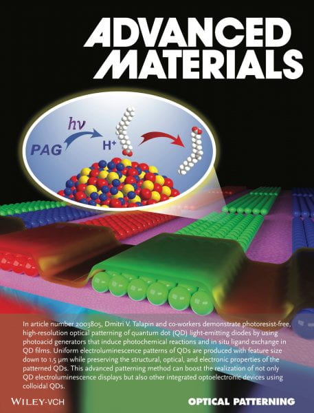

242. Area and thickness dependence of Auger recombination in nanoplatelets
John P. Philbin, Alexandra Brumberg, Benjamin T. Diroll, Wooje Cho, Dmitri V. Talapin, Richard D. Schaller, and Eran Rabani. J. Chem. Phys. 2020, 153, 054104.
Abstract

241. Covalent surface modifications and superconductivity of two-dimensional metal carbide MXenes
Vladislav Kamysbayev, Alexander S. Filatov, Huicheng Hu, Xue Rui, Francisco Lagunas, Di Wang, Robert F. Klie, and Dmitri V. Talapin. Science 2020, 369, 979.
UChicago News: UChicago chemists invent way to customize compounds just a few atoms thick
Abstract
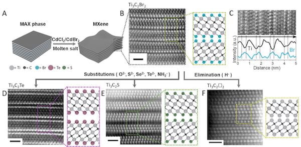
240. sasPDF: pair distribution function analysis of nanoparticle assemblies from small-angle scattering data
Chia-Hao Liu, Eric M. Janke, Ruipen Li, Pavol Juhás, Oleg Gang, Dmitri V. Talapin, and Simon J. L. Billinge. J. Appl. Cryst. 2020, 53, 699.
Abstract
239. Bright trion emission from semiconductor nanoplatelets
Lintao Peng, Matthew Otten, Abhijit Hazarika, Igor Coropceanu, Moritz Cygorek, Gary P. Wiederrecht, Pawel Hawrylak, Dmitri V. Talapin, and Xuedan Ma. Phys. Rev. Materials 2020, 4, 056006.
Abstract
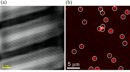
238. Heat-driven acoustic phonons in lamellar nanoplatelet assemblies
Benjamin T. Diroll, Vladislav Kamysbayev, Igor Coropceanu, Dmitri V. Talapin, and Richard D. Schaller. Nanoscale 2020, 12, 9661.
Abstract
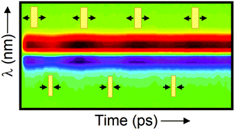
237. Nonequilibrium Thermodynamics of Colloidal Gold Nanocrystals Monitored by Ultrafast Electron Diffraction and Optical Scattering Microscopy
Burak Guzelturk, James K. Utterback, Igor Coropceanu, Vladislav Kamysbayev, Eric M. Janke, Marc Zajac, Nuri Yazdani, Benjamin L. Cotts, Suji Park, Aditya Sood, Ming-Fu Lin, Alexander H. Reid, Michael E. Kozina, Xiaozhe Shen, Stephen P. Weathersby, Vanessa Wood, Alberto Salleo, Xijie Wang, Dmitri V. Talapin, Naomi S. Ginsberg, and Aaron M. Lindenberg. ACS Nano 2020, 14, 4792.
Abstract

236. Quantized Reaction Pathways for Solution Synthesis of Colloidal ZnSe Nanostructures: A Connection between Clusters, Nanowires, and Two-Dimensional Nanoplatelets
P. D. Cunningham, Igor Coropceanu, K. Mulloy, W. Cho, D. V. Talapin. ACS Nano 2020, 14, 3847.
Abstract
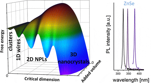
235. Quantum dot solids showing state-resolved band-like transport
X. Lan, M. Chen, M. H. Hudson, V. Kamysbayev, Y. Wang, P. Guyot-Sionnest, and D. V. Talapin. Nature Mater. 2020, 19, 323.
Abstract

234. Hot-Carrier Relaxation in CdSe/CdS Core/Shell Nanoplatelets
M. Pelton, Y, Wang, I. Fedin, D. V. Talapin, S. K. O’Leary. J. Phys. Chem. C 2020, 124, 1020.
Abstract
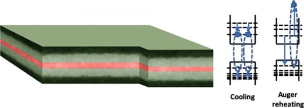
233. Titanium Nitride Modified Photoluminescence from Single Semiconductor Nanoplatelets
L. Peng, X. Wang, I. Coropceanu, A. B. Martinson, H. Wang, D. V. Talapin, and X. Ma. Adv. Funct. Mater. 2020, 30, 1904179.
Abstract
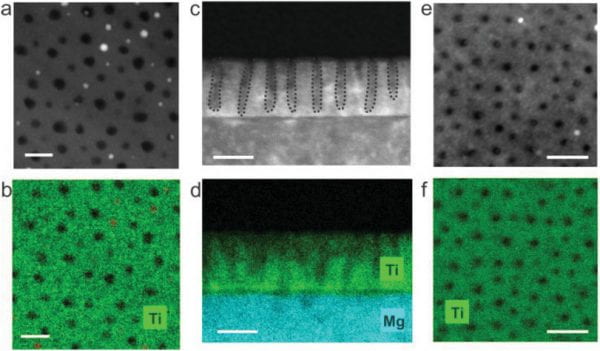
2019
232. Direct Wavelength-Selective Optical and Electron-Beam Lithography of Functional Inorganic Nanomaterials
Y. Wang, J.-A. Pan, H. Wu, and D. V. Talapin. ACS Nano 2019, 13, 13917.
Abstract
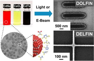
231. Colloidal Gelation in Liquid Metals Enables Functional Nanocomposites of 2D Metal Carbides (MXenes) and Lightweight Metals
V. Kamysbayev, N. M. James, A. S. Filatov, V. Srivastava, B. Anasori, H. M. Jaeger, Y. Gogotsi, and D. V. Talapin. ACS Nano 2019, 13, 12415.
Abstract
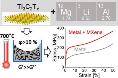
230. Polarized near-infrared intersubband absorptions in CdSe colloidal quantum wells
B. T. Diroll, M. Chen, I. Coropceanu, K. R. Williams, D. V. Talapin, P. Guyot-Sionnest, and R. D. Schaller. Nat. Commun. 2019, 10, 4511.
Abstract
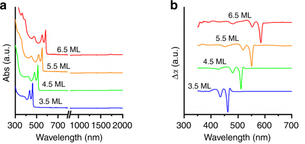
229. High Carrier Mobility in HgTe Quantum Dot Solids Improves Mid-IR Photodetectors
M. Chen, X. Lan, X. Tang, Y. Wang, M. H. Hudson, D. V. Talapin, and P. Guyot-Sionnest. ACS Photonics 2019, 6, 2358.
Abstract
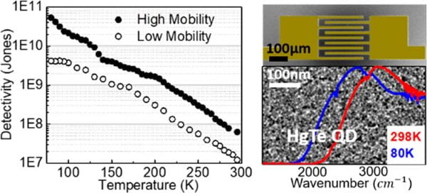
228. Colloidal Atomic Layer Deposition with Stationary Reactant Phases Enables Precise Synthesis of “Digital” II-VI Nano-heterostructures with Exquisite Control of Confinement and Strain
A. Hazarika, I. Fedin, L. Hong, J. Guo, V. Srivastava, W. Cho, I. Coropceanu, J. C. Portner, B. T. Diroll, J. P. Philbin, E. Rabani, R. F. Klie, and D. V. Talapin. J. Am. Chem. Soc. 2019, 141, 13487.
Abstract
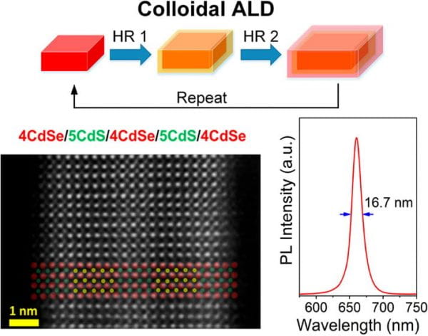
227. Uniaxial transition dipole moments in semiconductor quantum rings caused by broken rotational symmetry
N. F. Hartmann, M. Otten, I. Fedin, D. V. Talapin, M. Cygorek, P. Hawrylak, M. Korkusinski, S. Gray, A. Hartschuh, and X. Ma. Nat. Commun. 2019, 10, 3253.
Abstract
226. Binary Assembly of PbS and Au Nanocrystals: Patchy PbS Surface Ligand Coverage Stabilizes the CuAu Superlattice
M. Boles and D. V. Talapin. ACS Nano 2019, 13, 5375.
Abstract

225. Nanocrystals in Molten Salts and Ionic Liquids: Experimental Observation of Ionic Correlations Extending beyond the Debye Length
V. Kamysbayev, V. Srivastava, N. B. Ludwig, O. J. Borkiewicz, H. Zhang, J. Ilavsky, B. Lee, K. W. Chapman, S. Vaikuntanathan, D. V. Talapin. ACS Nano 2019, 13, 5760.
Abstract
224. Systematic Mapping of Binary Nanocrystal Superlattices: The Role of Topology in Phase Selection
I. Coropceanu, M. A. Boles, D. V. Talapin. J. Am. Chem. Soc. 2019, 141, 5728.
Abstract
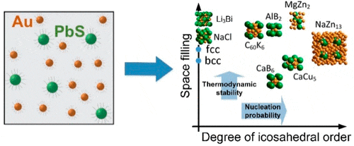
2018
223. Describing screening in dense ionic liquids with a charge-frustrated Ising model
N. B. Ludwig, K. Dasbiswas, D. V. Talapin, S. Vaikuntanathan. J. Chem. Phys. 2018, 149, 164505.
Abstract
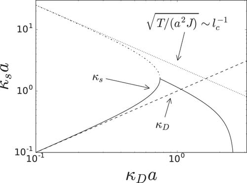
222. Origin of Broad Emission Spectra in InP Quantum Dots: Contributions from Structural and Electronic Disorder
E. M. Janke, N. E. Williams, C. She, D. Zherebetskyy, M. Hudson, L. Wang, D. J. Gosztola, R. D. Schaller, B. Lee, C. Sun, G. S. Engel, D. V. Talapin. J. Am. Chem. Soc. 2018, 140, 15791.
Abstract
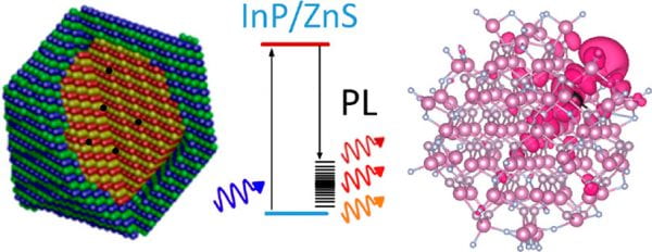
221. Direct Synthesis of Six-Monolayer (1.9 nm) Thick Zinc-Blende CdSe Nanoplatelets Emitting at 585 nm
W. Cho, S. Kim, I. Coropceanu, V. Srivastava, B. T. Diroll, A. Hazarika, I. Fedin, R. D. Schaller, G. Galli, D. V. Talapin. Chem. Mater. 2018, 30, 6957.
Abstract
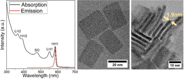
220. Semiconductor Nanoplatelet Excimers
B. T. Diroll, W. Cho, I. Coropceanu, S. Harvey, A. Brumberg, N. Holtgrewe, S. A. Crooker, M. R. Wasielewski, V. B. Prakapenka, D. V. Talapin, R. D. Schaller. Nano Lett. 2018, 18, 6948.
Abstract
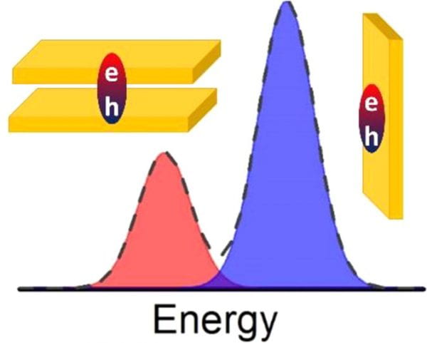
219. Colloidal Chemistry in Molten Salts: Synthesis of Luminescent In1–xGaxP and In1–xGaxAs Quantum Dots
V. Srivastava, V. Kamysbayev, L. Hong, E. Dunietz, R. F. Klie, D. V. Talapin. J. Am. Chem. Soc. 2018, 140, 12144.
Abstract
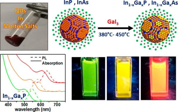
218. Conduction Band Fine Structure in Colloidal HgTe Quantum Dots
M. H. Hudson, M. Chen, V. Kamysbayev, E. M. Janke, X. Lan, G. Allan, C. Delerue, B. Lee, P. Guyot-Sionnest, D. V. Talapin. ACS Nano 2018, 12, 9397.
Abstract

217. Anisotropic photoluminescence from isotropic optical transition dipoles in semiconductor nanoplatelets
X. Ma, B. T. Diroll, W. Cho, I. Fedin, R. D. Schaller, D. V. Talapin, and G. P. Wiederrecht. Nano Lett. 2018, 18, 4647.
Abstract
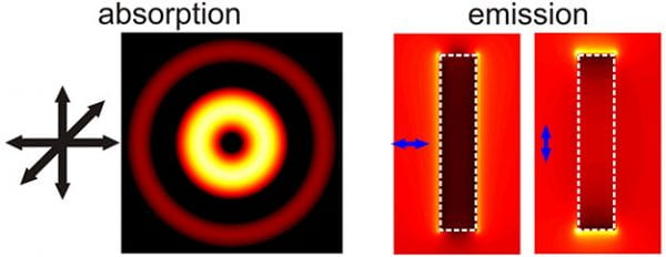
216. Surface chemistry and buried interfaces in all-inorganic nanocrystalline solids
E. Scalise, V. Srivastava, E. M. Janke, D. Talapin, G. Galli, and S. Wippermann. Nature Nanotech. 2018, 33, 841.
Abstract

215. Monodisperse InAs Quantum Dots from Aminoarsine Precursors: Understanding the Role of Reducing Agent
V. Srivastava, E. Dunietz, V. Kamysbayev, J. S. Anderson, and D. V. Talapin. Chem. Mater. 2018, 30, 3623.
Abstract
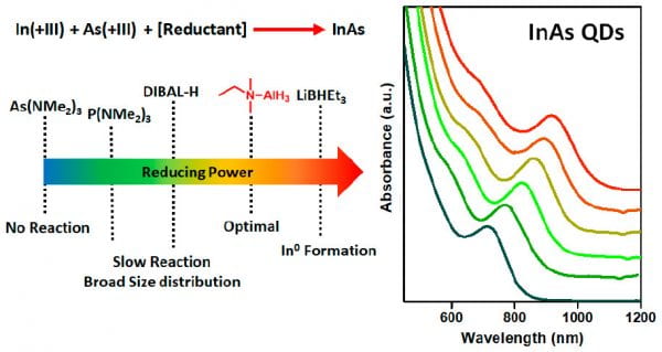
214. Elevated Temperature Photophysical Properties and Morphological Stability of CdSe and CdSe/CdS Nanoplatelets
C. E. Rowland, I. Fedin, B. T. Diroll, Y. Liu, D. V. Talapin, and R. D. Schaller. J. Phys. Chem. Lett. 2018, 9, 286.
Abstract
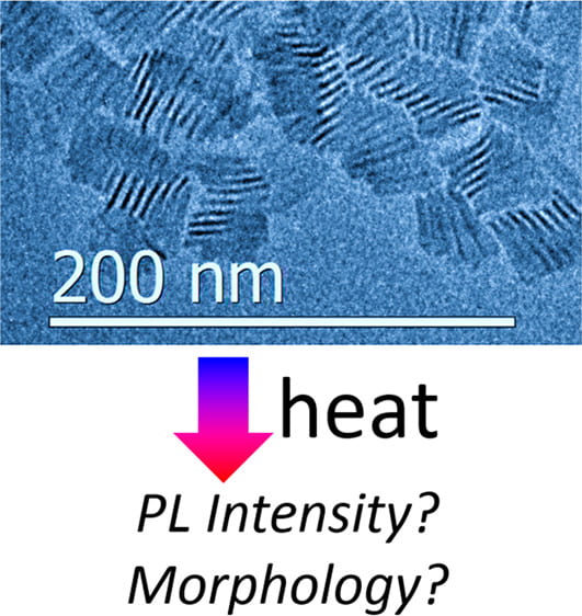
2017
213. Nonmonotonic Dependence of Auger Recombination Rate on Shell Thickness for CdSe/CdS Core/Shell Nanoplatelets
M. Pelton, J. J. Andrews, I. Fedin, D. V. Talapin, H. Lengd S. K. O’Leary. Nano Lett. 2017, 17, 6900.
Abstract
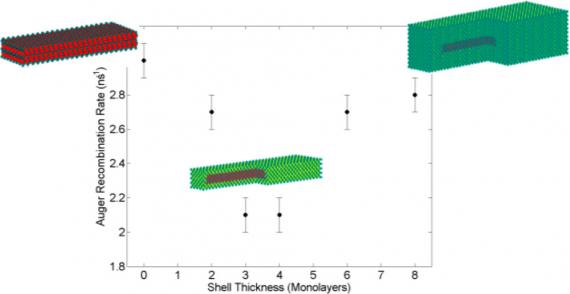
212. Size-Dependent Biexciton Quantum Yields and Carrier Dynamics of Quasi-Two-Dimensional Core/Shell Nanoplatelets
X. Ma, B. T. Diroll, W. Cho, I. Fedin, R. D. Schaller, D. V. Talapin, S. K. Gray, G. P. Wiederrecht, and D. J. Gosztola. ACS Nano 2017, 11, 9119.
Abstract

211. Direct optical lithography of functional inorganic nanomaterials
Y. Wang, I. Fedin, H. Zhang, and D. V. Talapin. Science 2017, 357, 385.
Perspective: M. Striccoli. Photolithography based on nanocrystals. Science 2017, 357, 353.
Abstract
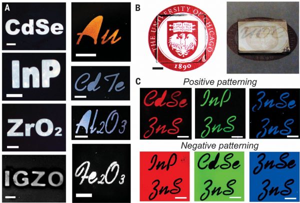
210. A room temperature continuous-wave nanolaser using colloidal quantum wells
Z. Yang, M. Pelton, I. Fedin, D. V. Talapin, and E. Waks. Nat. Commun. 2017, 8, 143.
Abstract
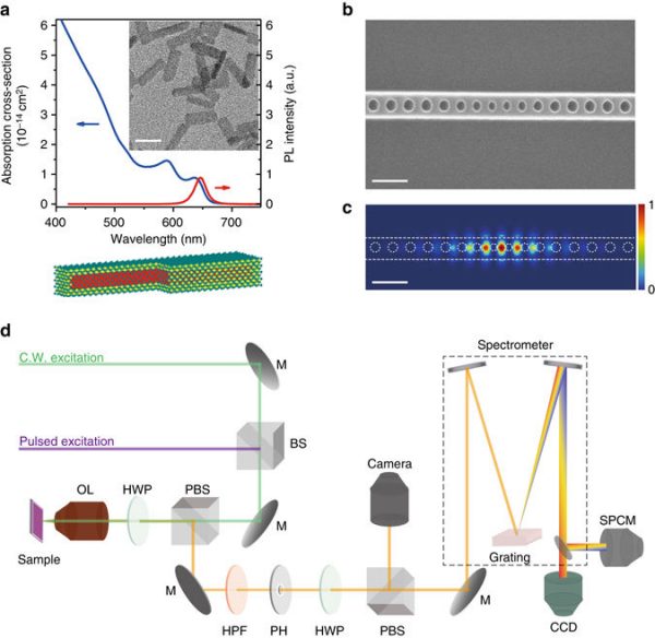
209. Soluble Lead and Bismuth Chalcogenidometallates: Versatile Solders for Thermoelectric Materials
H. Zhang, J. S. Son, D. S. Dolzhnikov, A. S. Filatov, A. Hazarika, Y. Wang, M. H. Hudson, C.-J. Sun, S. Chattopadhyay, and D. V. Talapin. Chem. Mater. 2017, 29, 6396.
Abstract
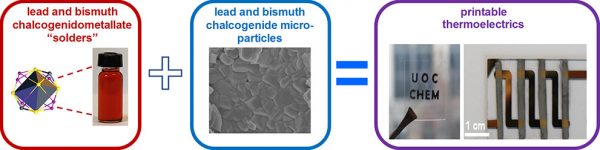
208. Orbitals, Occupation Numbers, and Band Structure of Short One-Dimensional Cadmium Telluride Polymers
A. J. S. Valentine, D. V. Talapin, and D. A. Mazziotti. J. Phys. Chem. A 2017, 121, 3142.
Abstract
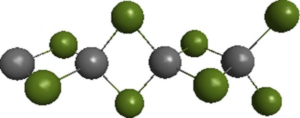
207. Stable colloids in molten inorganic salts
H. Zhang, K. Dasbiswas, N. B. Ludwig, G. Han, B. Lee, S. Vaikuntanathan, and D. V. Talapin. Nature 2017, 542, 328.
Abstract
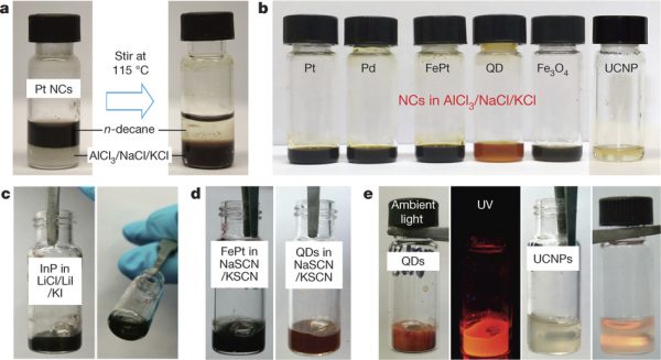
206. Understanding and curing structural defects in colloidal GaAs nanocrystals
V. Srivastava, W. Liu, E. M. Janke, V. Kamysbayev, A. S. Filatov, C. Sun, B. Lee, Tijana Rajh, R. D. Schaller, and D. V. Talapin. Nano Lett. 2017, 17, 2094.
Abstract
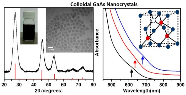
205. Violet-to-Blue Gain and Lasing from Colloidal CdS Nanoplatelets: Low-Threshold Stimulated Emission Despite Low Photoluminescence Quantum Yield
B. T. Diroll, D. V. Talapin, and R. D. Schaller. ACS Photonics 2017, 4, 576.
Abstract
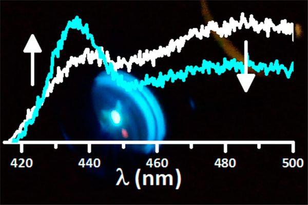
204. New forms of CdSe: molecular wires, gels, and ordered mesoporous assemblies
M. H. Hudson, D. S. Dolzhnikov, A. S. Filatov, E. M. Janke, J. Jang, B. Lee, C. Sun, and D. V. Talapin. J. Am. Chem. Soc. 2017, 139, 3368.
Abstract

203. Tandem Solar Cells from Solution-Processed CdTe and PbS Quantum Dots Using a ZnTe–ZnO Tunnel Junction
R. W. Crisp, G. F. Pach, J. M. Kurley, R. M. France, M. O. Reese, S. U. Nanayakkara, B. A. MacLeod, D. V. Talapin, M. C. Beard, and J. M. Luther. Nano Lett. 2017, 17, 1020.
Abstract
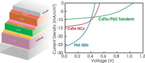
202. Transparent Ohmic Contacts for Solution-Processed, Ultrathin CdTe Solar Cells
J. M. Kurley, M. G. Panthani, R. W. Crisp, S. U. Nanayakkara, G. F. Pach, M. O. Reese, M. H. Hudson, D. S. Dolzhnikov, V. Tanygin, J. M. Luther, and D. V. Talapin. ACS Energy Lett. 2017, 2, 270.
Abstract