Publications Prior to 2009
2008
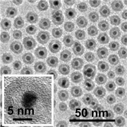
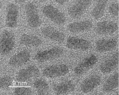
104. Gold/Iron Oxide Core/Hollow-Shell Nanoparticles
Elena V. Shevchenko, Maryna I. Bodnarchuk, Maksym V. Kovalenko, Dmitri V. Talapin, Rachel K. Smith, Shaul Aloni, Wolfgang Heiss, and A. Paul Alivisatos. Adv. Mater. 2008, 20, 4323.
Abstract
Gold/iron oxide core/hollow‐shell composite nanoparticles (NPs) with controllable shell thicknesses are synthesized (see figure). The gap between the Au core and iron oxide shell is formed as a result of different outward and inward diffusion rates of Fe and O, respectively. Control over interparticle interactions allows encapsulation of several Au cores inside one iron oxide shell. Superparamagnetic measurements of the NPs at room temperature demonstrate the plasmon resonance at 565 nm.
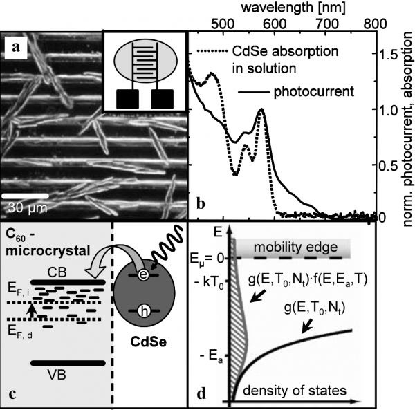
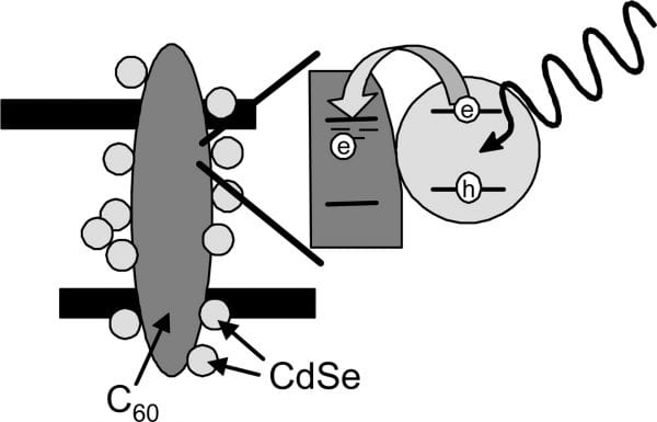
103. Photodoping with CdSe nanocrystals as a tool to prove trap-state distributions in C60 crystals
A. Biebersdorf, R. Dietmueller, A. Ohlinger, T. A. Klar, J. Feldmann, D. V. Talapin, and H. Weller. Appl. Phys. B 2008, 93, 239.
Abstract
We demonstrate the influence of
102. Au-PbS Core-Shell Nanocrystals: Plasmonic Absorption Enhancement and Electrical Doping via Interparticle Charge Transfer
Jong-Soo Lee, Elena V. Shevchenko, and Dmitri V. Talapin. J. Am. Chem. Soc. 2008, 130, 9673.
Abstract
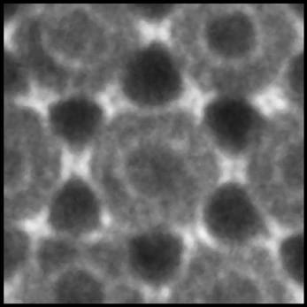
The discovery of quasicrystals in 1984 changed our view of ordered solids as periodic structures and introduced new long-range-ordered phases lacking any translational symmetry. Quasicrystals permit symmetry operations forbidden in classical crystallography, for example five-, eight-, ten- and 12-fold rotations, yet have sharp diffraction peaks. Intermetallic compounds have been observed to form both metastable and energetically stabilized quasicrystals; quasicrystalline order has also been reported for the tantalum telluride phase with an approximate Ta1.6Te composition. Later, quasicrystals were discovered in soft matter, namely supramolecular structures of organic dendrimers and tri-block copolymers, and micrometre-sized colloidal spheres have been arranged into quasicrystalline arrays by using intense laser beams that create quasi-periodic optical standing-wave patterns. Here we show that colloidal inorganic nanoparticles can self-assemble into binary aperiodic superlattices. We observe formation of assemblies with dodecagonal quasicrystalline order in different binary nanoparticle systems: 13.4-nm Fe2O3 and 5-nm Au nanocrystals, 12.6-nm Fe3O4 and 4.7-nm Au nanocrystals, and 9-nm PbS and 3-nm Pd nanocrystals. Such compositional flexibility indicates that the formation of quasicrystalline nanoparticle assemblies does not require a unique combination of interparticle interactions, but is a general sphere-packing phenomenon governed by the entropy and simple interparticle potentials. We also find that dodecagonal quasicrystalline superlattices can form low-defect interfaces with ordinary crystalline binary superlattices, using fragments of (33.42) Archimedean tiling as the ‘wetting layer’ between the periodic and aperiodic phases.
101. Self-assembly of semiconductor nanocrystals into ordered superstructures
E. V. Shevchenko and D. V. Talapin. In Semiconductor Nanocrystal Quantum Dots. A. L. Rogach, ed. Springer 2008, ISBN 978-3-211-75235-7.
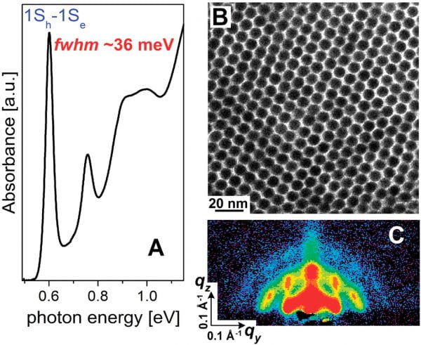
100. Enhanced Thermopower in PbSe Nanocrystal Quantum Dot Superlattices
R. Y. Wang, J. P. Feser, J.-S. Lee, D. V. Talapin, R. Segalman, and A. Majumdar. Nano Lett. 2008, 8, 2283.
Abstract
We examine the effect of strong three-dimensional quantum confinement on the thermopower and electrical conductivity of PbSe nanocrystal superlattices. We show that for comparable carrier concentrations PbSe nanocrystal superlattices exhibit a substantial thermopower enhancement of several hundred microvolts per Kelvin relative to bulk PbSe. We also find that thermopower increases monotonically as the nanocrystal size decreases due to changes in carrier concentration. Lastly, we demonstrate that thermopower of PbSe nanocrystal solids can be tailored by charge-transfer doping.
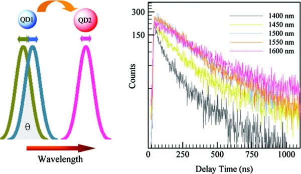
99. Temperature-Tuning of Near-Infrared Monodisperse Quantum Dot Solids at 1.5 µm for Controllable Forster Energy Transfer
R. Bose, J. F. McMillan, J. Gao, K. M. Rickey, C. J. Chen, D. V. Talapin, C. B. Murray, and C. W. Wong. Nano Lett. 2008, 8, 2006.
Abstract
We present the first time-resolved cryogenic observations of Förster energy transfer in large, monodisperse lead sulfide quantum dots with ground-state transitions near 1.5 µm (0.8 eV), in environments from 160 K to room temperature. The observed temperature-dependent dipole−dipole transfer rate occurs in the range of (30−50 ns)−1, measured with our confocal single-photon counting setup at 1.5 µm wavelengths. By temperature-tuning the dots, 94% efficiency of resonant energy transfer can be achieved for donor dots. The resonant transfer rates match well with proposed theoretical models.
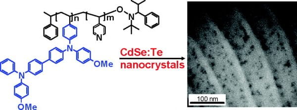
98. Semiconductor block copolymer nanocomposites with lamellar morphology via self-organization
S. Maria, A. S. Susha, M. Sommer, D. V. Talapin, A. L. Rogach, and M. Thelakkat. Macromolecules 2008, 41, 6081.
Abstract
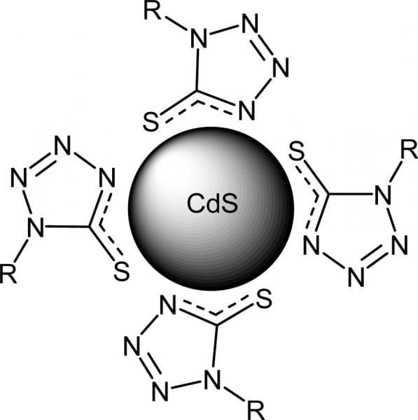
97. CdS Nanoparticles Capped with 1-Substituted 5-Thiotetrazoles: Synthesis, Characterization and Thermolysis of the Surfactant
S. V. Voitekhovich, D. V. Talapin, C. Klinke, A. Kornowski, and H. Weller. Chem. Mater. 2008, 20, 4545.
Abstract
96. LEGO Materials
D. V. Talapin. ACS Nano 2008, 2, 1097.
Abstract
95. Anisotropic optical emission of single CdSe/CdS tetrapod heterostructures; Evidence for a wavefunction symmetry breaking
C. Mauser, T. Limmer, E. Da Como, K. Becker, A. L. Rogach, J. Feldmann, and D. V. Talapin. Phys. Rev. B 2008, 77, 153303.
Abstract
Semiconductor tetrapods are expected to exhibit isotropic optical properties due to their tetrahedral symmetry. We have investigated the optical polarization properties of individual
tetrapods of high structural quality. In contrast to the light absorption behavior, a pronounced anisotropy is observed in the optical emission. This unexpected result can only be explained by assuming a symmetry breaking in the electronic wavefunction. Calculations reveal that slight differences between the arm diameters induce the polarized emission and a decrease in the photoluminescence intensity.
94. Quasi-Seeded Growth of Ligand-Tailored PbSe Nanocrystals through Cation-Exchange-Mediated Nucleation
M. V. Kovalenko, D. V. Talapin, M. A. Loi, F. Cordella, G. Hesser, M. I. Bodnarchuk, and W. Heiss. Angew. Chem. Int. Ed. 2008, 47, 3029.
Abstract
93. Self-Assembled Binary Superlattices of CdSe and Au Nanocrystals and Their Fluorescence Properties
E. V. Shevchenko, M. Ringler, A. Schwemer, D. V. Talapin, T. A. Klar, AL. Rogach, J. Feldmann, and A. Paul Alivisatos. J. Am. Chem. Soc. 2008, 130, 3274.
Abstract
2007
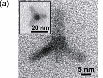
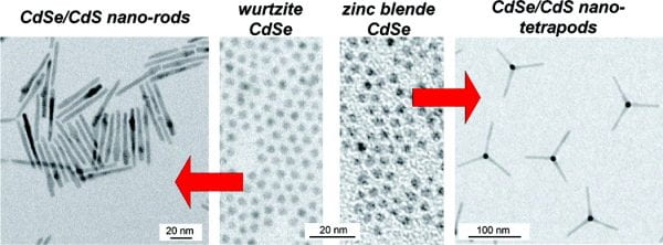
92. Seeded growth of highly luminescent CdSe/CdS nanoheterostructures with rod and tetrapod morphologies
D. V. Talapin, J. H. Nelson, E. V. Shevchenko, S. Aloni, B. Sadtler, and A. P. Alivisatos. Nano Lett. 2007, 7, 2951.
Abstract
We have demonstrated that seeded growth of nanocrystals offers a convenient way to design nanoheterostructures with complex shapes and morphologies by changing the crystalline structure of the seed. By using CdSe nanocrystals with wurtzite and zinc blende structure as seeds for growth of CdS nanorods, we synthesized CdSe/CdS heterostructure nanorods and nanotetrapods, respectively. Both of these structures showed excellent luminescent properties, combining high photoluminescence efficiency (∼80 and ∼50% for nanorods and nanotetrapods, correspondingly), giant extinction coefficients (∼2 × 10⁷ and ∼1.5 × 10⁸ M-1 cm-1 at 350 nm for nanorods and nanotetrapods, correspondingly), and efficient energy transfer from the CdS arms into the emitting CdSe core.
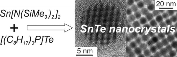
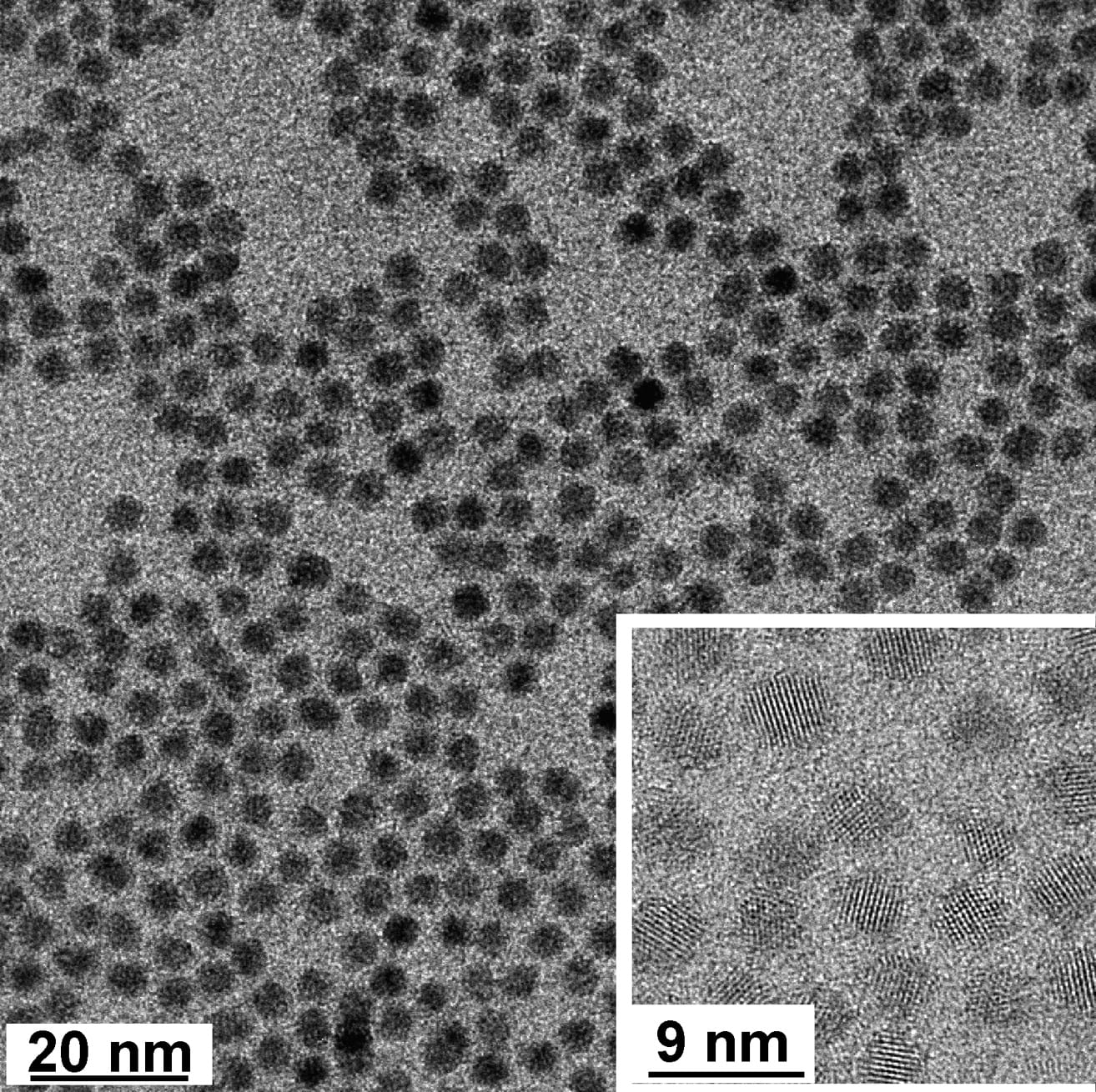
91. SnTe Nanocrystals: A New Example of Narrow Gap Semiconductor Quantum Dots
M. V. Kovalenko, W. Heiss, E. V. Shevchenko, J.-S. Lee, H. Schwinghammer, A. P. Alivisatos, and D. V. Talapin. J. Am. Chem. Soc. 2007, 129, 11354.
Abstract
A solution-phase synthesis of monodisperse SnTe nanocrystals via the reaction of bis[bis(trimethylsilyl)amino]tin(II) with trioctylphosphine telluride in oleylamine is demonstrated. The obtained SnTe nanocrystals are single-crystalline particles with a cubic rock-salt crystal structure. The size of the SnTe nanocrystals can be precisely tuned in the range of 4.5−15 nm by tailoring the reaction temperature and stabilizer concentration. These SnTe nanocrystals exhibit size-tunable band gap energies of 0.38−0.8 eV. The narrow size-distributions allow assembling SnTe nanocrystals into 3-dimensional superlattices.
90. Correlating Dynamics and Selectivity in Adsorption of Semiconductor Nanocrystals onto a Self-Organized Pattern
X. Chen, M. Hirtz, A. L. Rogach, D. V. Talapin, H. Fuchs, L. Chi. Nano Lett. 2007, 7, 3483.
Abstract
Selective adsorption of semiconductor nanocrystals onto an organic self-organized pattern shows a time-dependent behavior. By studying the wetting behavior of delivered solvent (1-phenyloctane) on a lipid self-organized pattern and determining the adhesion energy between semiconductor nanocrystals and substrate, we obtain a correlation between dynamics and selectivity in adsorption of semiconductor nanocrystals onto the pattern by constructing a potential energy landscape. Two consecutive steps for selective adsorption of nanocrystals onto the self-organized pattern have been established: the first one is the molecule exchange of 1-phenyloctane and lipid molecules to form the adsorption sites for nanocrystals, and the second one is the adsorption of nanocrystals onto the adsorption sites due to the strong interaction between nanocrystals and substrate.
89. Synthesis of Colloidal PbSe/PbS Core-Shell Nanowires and PbS/Au Nanowire-Nanocrystal Heterostructures
D. V. Talapin, H. Yu, E. V. Shevchenko, A. Lobo, and C. B. Murray. J. Phys. Chem. C 2007, 111, 14049.
Abstract
The oriented attachment of PbSe nanocrystals results in single-crystalline colloidal PbSe nanowires. The addition of different surfactants allows tailoring nanowire morphology, choosing between straight, zigzag, helical, and branched nanowires. In this work, we studied the formation of coaxial PbSe/PbS core−shell heterostructures and observed Stranski−Krastanov growth regime of PbS shell on PbSe nanowires at low reaction temperature (150 °C) that switched to layer-by-layer epitaxial growth above 180 °C. The protection of PbSe nanowires with a PbS shell substantially improves the nanowire stability against oxidation. We also developed a technique for controllable decoration of colloidal PbSe nanowires with Au nanoparticles and found that the morphology of nanowire template had a strong effect on nucleation and growth of gold nanoparticles.
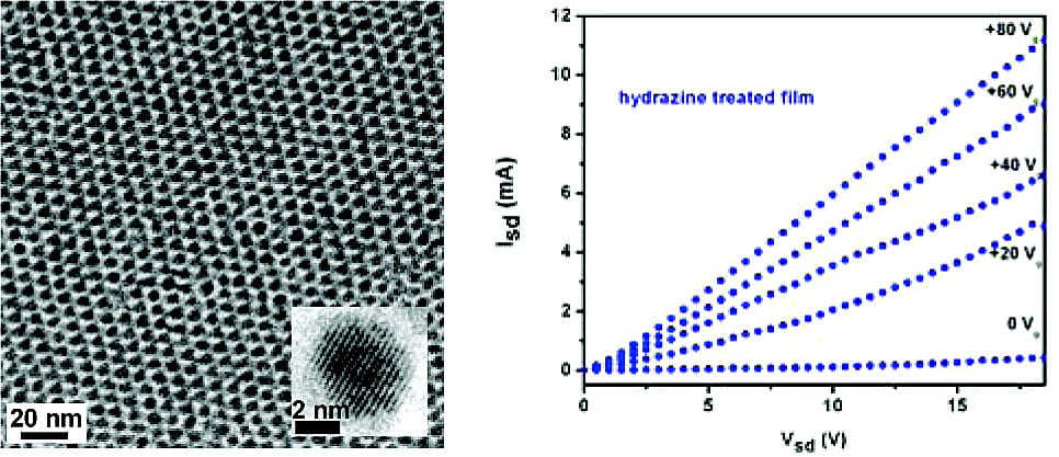
88. Alignment, Electronic Properties, Doping, and On-Chip Growth of Colloidal PbSe Nanowires
D. V. Talapin, C. T. Black, C. R. Kagan, E. V. Shevchenko, A. Afzali, and C. B. Murray. J. Phys. Chem. C 2007, 111, 13244.
Abstract
Single-crystalline straight, zigzag, helical, and branched nanowires can be synthesized by oriented attachment of PbSe nanocrystals followed by their fusion in the presence of different surfactants. These colloidal nanowires can be aligned in external electrical fields, facilitating their integration into electronic circuits. We show how the nanowire morphology affects the interaction of nanowires with the electric field. Conducting PbSe nanowires can be assembled from nanocrystal building blocks directly on a chip, growing along the electric field. As-formed PbSe nanowires show a p-type conduction that can be switched to an n-type by charge-transfer doping of the nanowires with hydrazine. In this work, we demonstrate strategies for device integration of solution-phase synthesized semiconductor nanowires and explore their electronic properties.
87. Quasi-ternary Nanoparticle Superlattices Through Nanoparticle Design
E. V. Shevchenko, J. Kortright, D. V. Talapin, S. Aloni, and A. P. Alivisatos. Adv. Mater. 2007, 19, 4183.
Abstract
Three component nanoparticle superlattices that are isostructural with binary ionic and intermetallic compounds are obtained by co‐crystallization of multi‐component nanoparticles (see figure). Self‐assembly of multicomponent nanoparticles greatly extends the combinations of possible materials types which can be intermixed on the nanoscale.
86. Time-Resolved Förster Energy Transfer from Individual Semiconductor Nanoantennae to Single Dye Molecules
D. Soujon, K. Becker, A. Rogach, J. Feldman, H. Weller, D. V. Talapin, and J. M. Lupton. J. Phys. Chem. C 2007, 111, 11511.
Abstract

85. Dipole−Dipole Interactions in Nanoparticle Superlattices
D. V. Talapin, E. V. Shevchenko, C. B. Murray, A. V. Titov, and P. Král. Nano Lett. 2007, 7, 1213.
Abstract

84. Synergism in binary nanocrystal superlattices leads to enhanced p-type conductivity in self-assembled PbTe/Ag2Te thin films
J. J. Urban, D. V. Talapin, E. V. Shevchenko, C. R. Kagan, and C. B. Murray. Nat. Mater. 2007, 6, 115.
Abstract

83. Resonant energy transfer within a colloidal nanocrystal polymer host system
S. Kaufmann, T. Stöferle, N. Moll, R. F. Mahrt, U. Scherf, A. Tsami, D. V. Talapin, and C. B. Murray. Appl. Phys. Lett. 2007, 90, 071108.
Abstract
Semiconductor tetrapods are expected to exhibit isotropic optical properties due to their tetrahedral symmetry. We have investigated the optical polarization properties of individual
tetrapods of high structural quality. In contrast to the light absorption behavior, a pronounced anisotropy is observed in the optical emission. This unexpected result can only be explained by assuming a symmetry breaking in the electronic wavefunction. Calculations reveal that slight differences between the arm diameters induce the polarized emission and a decrease in the photoluminescence intensity.
82. CdSe:Te Nanocrystals: Band-Edge versus Te-Related Emission
T. Franzl, J. Müller, T. A. Klar, A. L. Rogach, J. Feldmann, D. V. Talapin, and H. Weller. J. Phys. Chem. C 2007, 111, 2974.
Abstract

81. White organic light-emitting devices incorporating nanoparticles of II–VI semiconductors
J. H. Ahn, C. Bertoni, S. Dunn, C. Wang, D. V. Talapin, N. Gaponik, A. Eychmuller, Y. Hua, M. R. Bryce, and M. C. Petty. Nanotechnology 2007, 33, 335202.
Abstract
80. Room Temperature Exciton Storage in Elongated Semiconductor Nanocrystals
R. M. Kraus, P. G. Lagoudakis, A. L. Rogach, D. V. Talapin, H. Weller, J. M. Lupton, J. Feldmann. Phys. Rev. Lett. 2007, 98, 017401.
Abstract
2006
79. Electrical control of Förster energy transfer
K. Becker, J. M. Lupton, J. Müller, A. L. Rogach, D. V. Talapin, H. Weller, and J. Feldmann. Nat. Mater. 2006, 5, 777.
Abstract
We have demonstrated that seeded growth of nanocrystals offers a convenient way to design nanoheterostructures with complex shapes and morphologies by changing the crystalline structure of the seed. By using CdSe nanocrystals with wurtzite and zinc blende structure as seeds for growth of CdS nanorods, we synthesized CdSe/CdS heterostructure nanorods and nanotetrapods, respectively. Both of these structures showed excellent luminescent properties, combining high photoluminescence efficiency (∼80 and ∼50% for nanorods and nanotetrapods, correspondingly), giant extinction coefficients (∼2 × 10⁷ and ∼1.5 × 10⁸ M-1 cm-1 at 350 nm for nanorods and nanotetrapods, correspondingly), and efficient energy transfer from the CdS arms into the emitting CdSe core.

78. Hierarchical Luminescence Patterning Based on Multiscaled Self-Assembly
X. Chen, A. L. Rogach, D. V. Talapin, H. Fuchs, and L. Chi. J. Am. Chem. Soc. 2006, 128, 9592.
Abstract
This communication describes a procedure for fabrication of hierarchical luminescence patterns based on the template-assisted assembly of CdSe nanocrystals on a self-assembled structure with green-emitting microstripes, as well as the photoinduced fluorescence enhancement of CdSe nanocrystals and photobleaching of dyes. The technique is low-cost and high-throughput and can be extended to many material combinations.
77. Semiconductor Nanocrystals Photosensitize C60 Crystals
A. Biebersdorf, R. Dietmüller, A. S. Susha, A. L. Rogach, S. K. Poznyak, D. V. Talapin, H. Weller, T. A. Klar, and J. Feldmann. Nano Lett. 2006, 6, 1559.
Abstract
Semiconductor nanocrystals (SCNCs) made of CdSe, CdTe, and InP are used to photosensitize needlelike C60 crystals. The photocurrent is increased by up to 3 orders of magnitude as compared with C60 crystals without SCNCs. The photocurrent spectrum can be tuned precisely by the SCNC size and material, rendering the SCNC-functionalized C60 crystals an excellent material for spectrally tuneable photodetectors. We explain the increased photocurrent as a result of photoexcited electrons transferring from the SCNCs to the C60 crystals and causing photoconductivity, while the complementary holes remain trapped in the SCNCs.
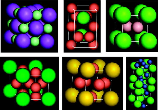
76. Structural Diversity in Binary Nanoparticle Superlattices
E. V. Shevchenko, D. V. Talapin, N. A. Kotov, S. O’Brien, and C. B. Murray. Nature 2006, 439, 55.
Highlights:
Nano Building Made Easy
Mixing nanoparticles for a variety of structures
Plenty of room at the top
Colloids get complex
Colloidal particles crystallize in an increasingly wide range of structures
A Periodic Table of Nanoparticles
New Families of Self-Assembled Nanolattices Created
Abstract
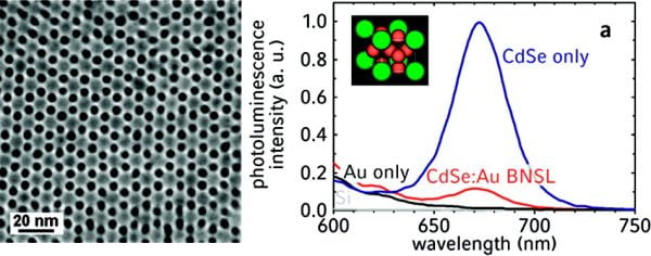
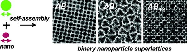
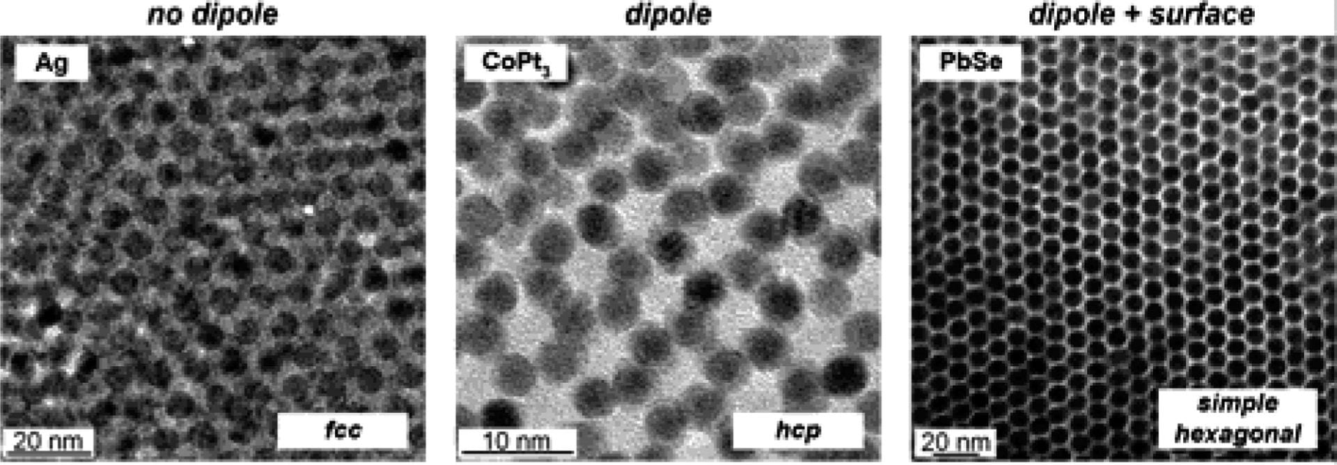
Assembly of small building blocks such as atoms, molecules and nanoparticles into macroscopic structures—that is, ‘bottom up’ assembly—is a theme that runs through chemistry, biology and material science. Bacteria, macromolecules and nanoparticles can self-assemble, generating ordered structures with a precision that challenges current lithographic techniques. The assembly of nanoparticles of two different materials into a binary nanoparticle superlattice (BNSL) can provide a general and inexpensive path to a large variety of materials (metamaterials) with precisely controlled chemical composition and tight placement of the components. Maximization of the nanoparticle packing density has been proposed as the driving force for BNSL formation, and only a few BNSL structures have been predicted to be thermodynamically stable. Recently, colloidal crystals with micrometre-scale lattice spacings have been grown from oppositely charged polymethyl methacrylate spheres. Here we demonstrate formation of more than 15 different BNSL structures, using combinations of semiconducting, metallic and magnetic nanoparticle building blocks. At least ten of these colloidal crystalline structures have not been reported previously. We demonstrate that electrical charges on sterically stabilized nanoparticles determine BNSL stoichiometry; additional contributions from entropic, van der Waals, steric and dipolar forces stabilize the variety of BNSL structures.

75. Structural Characterization of Self-Assembled Multifunctional Binary Nanoparticle Superlattices
E. V. Shevchenko, D. V. Talapin, C. B. Murray, and S. O’Brien. J. Am. Chem. Soc. 2006, 128, 3620.
Abstract
Nanocrystals of different size and functionality (e.g., noble metals, semiconductors, oxides, magnetic alloys) can be induced to self-assemble into ordered binary superlattices (also known as opals or colloidal crystals), retaining the size tunable properties of their constituents. We have built a variety of binary superlattices from monodisperse PbS, PbSe, CoPt3, Fe2O3, Au, Ag, and Pd nanocrystals, mixing and matching these nanoscale building blocks to yield multifunctional nanocomposites (metamaterials). Superlattices with AB, AB2, AB3, AB4, AB5, AB6, and AB13 stoichiometry with cubic, hexagonal, tetragonal, and orthorhombic symmetries have been identified. Assemblies with the same stoichiometry can be produced in several polymorphous forms by tailoring the particle size and deposition conditions. We have identified arrays isostructural with NaCl, CuAu, AlB2, MgZn2, MgNi2, Cu3Au, Fe4C, CaCu5, CaB6, NaZn13, and cub-AB13 compounds emphasizing the parallels between nanoparticle assembly and atomic scale crystal growth and providing confidence that many more structures will follow. Recently, we have demonstrated that electrical charges on sterically stabilized nanoparticles in addition to such parameters as particle size ratio and their concentrations can provide the formation of a much broader pallet of binary nanoparticle superlattices1 as compared with the limited number of possible superlattices formed by hard noninteracting spheres. In this contribution, we demonstrate a large variety of different binary superlattices, provide their detailed structural characterization, and discuss the role of energetic and kinetic factors in the cocrystallization process. We found that Coulomb, van der Waals, charge−dipole, dipole−dipole, and other interactions can contribute equally to cocrystallization, allowing superlattice formation to be dependent on a number of tunable parameters. We present binary superlattices as a new class of materials with a potentially unlimited library of constituents over a wide range of tunable structures.
74. Self-Assembly of PbTe Quantum Dots into Nanocrystal Superlattices and Glassy Films
J. J. Urban, D. V. Talapin, E. V. Shevchenko, and C. B. Murray. J. Am. Chem. Soc. 2006, 128, 3248.
Abstract
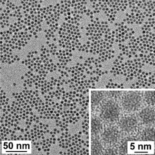
Monodisperse lead telluride (PbTe) nanocrystals ranging from ∼4 to 10 nm in diameter are synthesized to provide quantum dot building blocks for the design of novel materials for electronic applications. Two complementary synthetic approaches are developed that enable either (1) isolation of small quantities of nanocrystals of many different sizes or (2) the production of up to 10 g of a single nanocrystal size. PbTe nanocrystals are characterized by transmission electron microscopy (TEM), X-ray diffraction (XRD), and optical absorption. Assembly of PbTe nanocrystals is directed to prepare nanocrystal solids that display either short-range (glassy solids) or long-range (superlattices) packing order by varying deposition conditions. Film order and average interparticle spacing are analyzed with grazing-incidence small-angle X-ray scattering (GISAXS) and high-resolution scanning electron microscopy (HRSEM). We perform the first optical and electronic studies of PbTe solids and demonstrate that chemical activation of these films enhances conductivity by ∼9−10 orders of magnitude while preserving their quantum dot nature.

73. Surface oxidation of CdTe nanocrystals—A high resolution core-level photoelectron spectroscopy study
A. Lobo, H. Borchert, D.V. Talapin, H. Weller, and T. Möller. Colloids and Surfaces A 2006, 286, 1.
Abstract
2005
72. PbSe Nanocrystal Solids for n- and p-Channel Thin Film Field-Effect Transistors
D. V. Talapin and C. B. Murray. Science 2005, 310, 86.
Highlights:
Turning insulating nanocrystal films into semiconductors
Abstract
Initially poorly conducting PbSe nanocrystal solids (quantum dot arrays or superlattices) can be chemically “activated” to fabricate n- and p-channel field effect transistors with electron and hole mobilities of 0.9 and 0.2 square centimeters per volt-second, respectively; with current modulations of about 103 to 104; and with current density approaching 3 × 10⁴amperes per square centimeter. Chemical treatments engineer the interparticle spacing, electronic coupling, and doping while passivating electronic traps. These nanocrystal field-effect transistors allow reversible switching between n- and p-transport, providing options for complementary metal oxide semiconductor circuits and enabling a range of low-cost, large-area electronic, optoelectronic, thermoelectric, and sensing applications.
71. Monitoring surface charge migration in the spectral dynamics of single Cd Se ∕ Cd S nanodot/nanorod heterostructures
J. Müller, J. M. Lupton, A. L. Rogach, J. Feldmann, D. V. Talapin, and H. Weller. Phys. Rev. B. 2005, 72, 205339.
Abstract
This communication describes a procedure for fabrication of hierarchical luminescence patterns based on the template-assisted assembly of CdSe nanocrystals on a self-assembled structure with green-emitting microstripes, as well as the photoinduced fluorescence enhancement of CdSe nanocrystals and photobleaching of dyes. The technique is low-cost and high-throughput and can be extended to many material combinations.

70. Wavefunction engineering in elongated semiconductor nanocrystals with heterogeneous carrier confinement
J. Müller, J. M. Lupton, P. G. Lagoudakis, R. Koeppe, A. L. Rogach, J. Feldmann, D. V. Talapin, and H. Weller. Nano Lett. 2005, 5, 2044.
Abstract
We explore two routes to wave function engineering in elongated colloidal CdSe/CdS quantum dots, providing deep insight into the intrinsic physics of these low-dimensional heterostructures. Varying the aspect ratio of the nanoparticle allows control over the electron−hole overlap (radiative rate), and external electric fields manipulate the interaction between the delocalized electron and the localized hole. In agreement with theory, this leads to an exceptional size dependent quantum confined Stark effect with field induced intensity modulations, opening applications as electrically switchable single photon sources.

69. Polarized-Light-Emitting Quantum-Rod Diodes.
R. A. M. Hikmet, P. T. K. Chin, D. V. Talapin, and H. Weller. Adv. Mater. 2005, 17, 1436.
Abstract
For the first time, polarized‐light‐emitting quantum‐rod diodes have been successfully produced, using thin layers of quantum rods oriented by a rubbing technique. Diode emission at 620 nm with a luminance efficiency of 0.65 Cd A–1 and an external quantum efficiency of 0.49 % is obtained.
68. Designing PbSe Nanowires and Nanorings through Oriented Attachment of Nanoparticles
K.-S. Cho, D. V. Talapin, W. Gaschler, C. B. Murray. J. Am. Chem. Soc. 2005, 127, 7140
Abstract
Nanocrystals of different size and functionality (e.g., noble metals, semiconductors, oxides, magnetic alloys) can be induced to self-assemble into ordered binary superlattices (also known as opals or colloidal crystals), retaining the size tunable properties of their constituents. We have built a variety of binary superlattices from monodisperse PbS, PbSe, CoPt3, Fe2O3, Au, Ag, and Pd nanocrystals, mixing and matching these nanoscale building blocks to yield multifunctional nanocomposites (metamaterials). Superlattices with AB, AB2, AB3, AB4, AB5, AB6, and AB13 stoichiometry with cubic, hexagonal, tetragonal, and orthorhombic symmetries have been identified. Assemblies with the same stoichiometry can be produced in several polymorphous forms by tailoring the particle size and deposition conditions. We have identified arrays isostructural with NaCl, CuAu, AlB2, MgZn2, MgNi2, Cu3Au, Fe4C, CaCu5, CaB6, NaZn13, and cub-AB13 compounds emphasizing the parallels between nanoparticle assembly and atomic scale crystal growth and providing confidence that many more structures will follow. Recently, we have demonstrated that electrical charges on sterically stabilized nanoparticles in addition to such parameters as particle size ratio and their concentrations can provide the formation of a much broader pallet of binary nanoparticle superlattices1 as compared with the limited number of possible superlattices formed by hard noninteracting spheres. In this contribution, we demonstrate a large variety of different binary superlattices, provide their detailed structural characterization, and discuss the role of energetic and kinetic factors in the cocrystallization process. We found that Coulomb, van der Waals, charge−dipole, dipole−dipole, and other interactions can contribute equally to cocrystallization, allowing superlattice formation to be dependent on a number of tunable parameters. We present binary superlattices as a new class of materials with a potentially unlimited library of constituents over a wide range of tunable structures.
74. Self-Assembly of PbTe Quantum Dots into Nanocrystal Superlattices and Glassy Films.
J. J. Urban, D. V. Talapin, E. V. Shevchenko, and C. B. Murray. J. Am. Chem. Soc. 2006, 128, 3248.
Abstract
Monodisperse lead telluride (PbTe) nanocrystals ranging from ∼4 to 10 nm in diameter are synthesized to provide quantum dot building blocks for the design of novel materials for electronic applications. Two complementary synthetic approaches are developed that enable either (1) isolation of small quantities of nanocrystals of many different sizes or (2) the production of up to 10 g of a single nanocrystal size. PbTe nanocrystals are characterized by transmission electron microscopy (TEM), X-ray diffraction (XRD), and optical absorption. Assembly of PbTe nanocrystals is directed to prepare nanocrystal solids that display either short-range (glassy solids) or long-range (superlattices) packing order by varying deposition conditions. Film order and average interparticle spacing are analyzed with grazing-incidence small-angle X-ray scattering (GISAXS) and high-resolution scanning electron microscopy (HRSEM). We perform the first optical and electronic studies of PbTe solids and demonstrate that chemical activation of these films enhances conductivity by ∼9−10 orders of magnitude while preserving their quantum dot nature.
73. Surface oxidation of CdTe nanocrystals—A high resolution core-level photoelectron spectroscopy study.
A. Lobo, H. Borchert, D.V. Talapin, H. Weller, and T. Möller. Colloids and Surfaces A 2006, 286, 1.
Abstract
85. Dipole−Dipole Interactions in Nanoparticle Superlattices
D. V. Talapin, E. V. Shevchenko, C. B. Murray, A. V. Titov, and P. Král. Nano Lett. 2007, 7, 1213.
Abstract
84. Synergism in binary nanocrystal superlattices leads to enhanced p-type conductivity in self-assembled PbTe/Ag2Te thin films
J. J. Urban, D. V. Talapin, E. V. Shevchenko, C. R. Kagan, and C. B. Murray. Nat. Mater. 2007, 6, 115.
Abstract
83. Resonant energy transfer within a colloidal nanocrystal polymer host system
S. Kaufmann, T. Stöferle, N. Moll, R. F. Mahrt, U. Scherf, A. Tsami, D. V. Talapin, and C. B. Murray. Appl. Phys. Lett. 2007, 90, 071108.
Abstract
Semiconductor tetrapods are expected to exhibit isotropic optical properties due to their tetrahedral symmetry. We have investigated the optical polarization properties of individual
tetrapods of high structural quality. In contrast to the light absorption behavior, a pronounced anisotropy is observed in the optical emission. This unexpected result can only be explained by assuming a symmetry breaking in the electronic wavefunction. Calculations reveal that slight differences between the arm diameters induce the polarized emission and a decrease in the photoluminescence intensity.
82. CdSe:Te Nanocrystals: Band-Edge versus Te-Related Emission
T. Franzl, J. Müller, T. A. Klar, A. L. Rogach, J. Feldmann, D. V. Talapin, and H. Weller. J. Phys. Chem. C 2007, 111, 2974.
Abstract
81. White organic light-emitting devices incorporating nanoparticles of II–VI semiconductors
J. H. Ahn, C. Bertoni, S. Dunn, C. Wang, D. V. Talapin, N. Gaponik, A. Eychmuller, Y. Hua, M. R. Bryce, and M. C. Petty. Nanotechnology 2007, 33, 335202.
Abstract
2005
67. Polymorphism in AB13nanoparticle superlattices: an example of semiconductor-metal metamaterials. E. V. Shevchenko, D. V. Talapin, S. O’Brien, C. B. Murray. J. Am. Chem. Soc.2005, v. 127, pp. 8741-8747.
Highlight: Nature Materials2005, v. 4, p.509.
66.Interplay between Auger and Ionization Processes in Nanocrystal Quantum Dots. R. M. Kraus, P. G. Lagoudakis, J. Mueller, A. L. Rogach, J. M. Lupton, J. Feldmann, D. V. Talapin, H. Weller. J. Phys. Chem. B. 2005, v.109,pp. 18214-18217.
65. The effect of nanocrystal surface structure on the luminescence properties: photoemission study of HF-etched InP nanocrystals. S. Adam, D. V. Talapin, H. Borchert, A. Lobo, C. McGinley, A. R. B. de Castro, M. Haase, H. Weller, T. Möller. J. Chem. Phys. 2005, v. 123, pp. 084706.
64. Self-assembly of monodisperse nanocrystals into facetted crystal superlattices. D. V. Talapin, E. V. Shevchenko, N. Gaponik, I. L. Radtchenko, A. Kornowski, M. Haase, A. L. Rogach, H. Weller. Adv. Mater.2005, v. 17, pp. 1325-1329.
63. Electrochemical oxidation of titanium by pulsed discharge in electrolyte. S. K. Poznyak, D. V. Talapin, A. I. Kulak. J. Electroanal. Chem.2005, v. 579, pp. 299-310.
62.Magnetic Nanocrystals and Their Superstructures. E. V. Shevchenko, D. V. Talapin, A. L. Rogach, H. Weller. in: Nanoparticle Assemblies and Superstructures, Ed.: N. A. Kotov, Marcel Dekker Ltd., 2005.
61. Size-dependent electrochemical behavior of thiol capped CdTe nanocrystals in aqueous solution. S. K. Poznyak, N. P. Osipovich, A. Shavel, D. V. Talapin, M. Gao, A. Eychmüller, N. Gaponik. J. Phys. Chem. B. 2005, vol. 109, pp. 1094-1100.
2004
60. CdSe/CdS/ZnS and CdSe/ZnSe/ZnS core-shell-shell nanocrystals. D. V. Talapin, I. Mekis, S. Götzinger,A. Kornowski, O. Benson,and H. Weller. J. Phys. Chem. B. 2004, vol. 108, pp.18826-18831.
Editors’ ChoiceScience 2004, vol. 306, p. 1439.
59. Monitoring surface charge movement in single elongated semiconductor nanocrystals. J. Müller, J. M. Lupton, A. L. Rogach, J. Feldmann, D. V. Talapin, H. Weller. Phys. Rev. Lett.2004, vol. 93, pp.167402-1 – 167402-4.
58. CdSe and CdSe/CdS nanorod solids. D. V. Talapin, E. V. Shevchenko, C. B. Murray, A. Kornowski, S. Förster and H. Weller.J. Am. Chem. Soc.2004,vol. 126,pp. 12984-12988.
Highlight: C. Sealy. Solid approach to Self-Assembly. Materials Today. 2004 v.7, no12, p.14.
57. Lateral Patterning of Luminescent CdSe Nanocrystals by Selective Dewetting from Self-Assembled Organic Templates. N. Lu, X. Chen, D. Molenda, A. Naber, H. Fuchs, D. V. Talapin, H. Weller, J. Müller, J. M. Lupton, J. Feldmann, A. L. Rogach, L. Chi. NanoLetters, 2004, vol. 4, pp.885-888.
56. Quantum Dot Chemiluminescence. S. K. Poznyak, D. V. Talapin, E. V. Shevchenko, H. Weller. NanoLetters, 2004, vol. 4, pp. 693-698.
55. Highly directional emission from colloidally synthesized nanocrystals in vertical cavities with small mode spacing. J. Roither, W. Heiss, D. V. Talapin, N. Gaponik, A. Eychmuller.Appl. Phys. Lett. 2004, vol 84, p. 2223.
54. Formation of Nanoparticle Arrays on S-Layer Protein Lattices. E. Györvary, A. Schroedter, D. V. Talapin, H. Weller, D. Pum, U. B. Sleytr. J. Nanoscience and Nanotechnology2004, vol. 4, pp.115-120.
53. Confocal microscopy and spectroscopy of nanocrystals on a high-Q microsphere resonator. S. Götzinger, L. de S. Menezes, O. Benson, D. V. Talapin, N. Gaponik, H. Weller, A. L. Rogach and V. Sandoghdar. J. Opt. B: Quantum Semiclass. Opt.2004, vol. 6pp.154–158.
52. Semiconductor Nanoparticles.A. L. Rogach, D. V. Talapin, H. Weller In “Colloids and Colloidal Assemblies” Ed. F. Caruso, WILEY VCH, Weinheim, 2004. pp.52-95.
51.Core-level photoemission study of the InAs/CdSe nanocrystalline system. C. McGinley, H. Borchert, D. V. Talapin, S. Adam, A. Lobo, A. R. B. de Castro, M. Haase, H. Weller, and T. Möller. Phys. Rev. B, 2004, vol. 69, p. 045301.
50. Air-induced fluorescence bursts from single semiconductor nanocrystals. J. Muller, J. M. Lupton, A. L. Rogach, J. Feldmann, D. V. Talapin, H. Weller. Appl. Phys. Lett.2004, vol. 85, pp. 381-383.
49. Photogeneration of charge carriers in blends of conjugated polymers and semiconducting nanoparticles. M. Pientka, J. Wisch, S. Boeger, J. Parisi, V. Dyakonov, A. Rogach, D. Talapin, H. Weller. Thin Solid Films 2004, vol. 451-452, pp. 48-53.
2003
48. Highly emissive colloidal CdSe/CdS heterostructures of mixed dimensionality.D. V. Talapin, R. Koeppe, S. Götzinger, A. Kornowski, J. M. Lupton, A. L. Rogach, O. Benson, J. Feldmann, H. Weller. NanoLetters, 2003, vol. 3, pp.1677-1681.
Editors’ ChoiceScience 2003, vol. 302, p. 1117.
47.Effect of ZnS shell thickness on the phonon spectra in CdSe quantum dots. A. V. Baranov, Yu. P. Rakovich, J. F. Donegan, T. S. Perova, R. A. Moore, D. V. Talapin, A.L. Rogach, Y. Masumoto, I. Nabiev. Phys. Rev. B, 2003, vol. 68, p.165306.
46. A study of conduction mechanism and electroluminescence in the PEDOT:PSS – CdSe/ZnS quantumdot composites. R.A.M Hikmet, D.V. Talapin, H. Weller. J. Appl. Phys. 2003, vol. 93, pp. 3509-3514.
45. Study of nucleation and growth in the hot organometallic synthesis of magnetic alloy nanocrystals: the role of nucleation rate in size control of CoPt3 nanocrystals. E. V. Shevchenko, D. V. Talapin, H. Schnablegger, A. Kornowski, M. Haase, H. Weller. J. Am. Chem. Soc.2003,vol. 125,pp. 9090-9101.
44. Synthesis and characterization of magnetic nanoparticles. D. V. Talapin, E. V. Shevchenko, H. Weller. In “Nanoparticles – from Theory to Applications.” Ed. G. Schmid, WILEY VCH, 2003, ISBN: 3-527-30507-6.
43. Self-assembly of Metal Nanoparticles. G. Schmid, D. V. Talapin, and E. V. Shevchenko. In “Nanoparticles – from Theory to Applications.” Ed. G. Schmid, WILEY VCH, 2003, ISBN: 3-527-30507-6.
42. Relations between the Photoluminescence Efficiency of CdTe Nanocrystals and their Surface Properties revealed by Synchrotron XPS. H. Borchert, D. V. Talapin, N. Gaponik, C. McGinley, S. Adam, A. Lobo, T. Möller, H. Weller. J. Phys. Chem. B2003, vol. 107, p. 9662.
41. Up-conversion luminescence via a below-gap state in CdSe/ZnS quantum dots. Yu.P. Rakovich, J.F. Donegana, S.A. Filonovich, M.J.M. Gomes, D.V. Talapin, A.L. Rogach, A. Eychmüller. Physica E2003, vol. 17, pp. 99 – 100.
40. Photoemission study of size selected InP nanocrystals: The relationship between luminescence yield and surface structure. S. Adam, C. McGinley, T. Möller, D. V. Talapin, H. Borchert, M. Haase, H. Weller. Eur. J. Phys. D2003, vol. 24, pp. 373-376.
39. One-pot synthesis of highly luminescent CdSe/CdS core-shell nanocrystals via organometallic and “greener” chemical approaches. I. Mekis, D. V. Talapin, A. Kornowski, M. Haase, H.Weller. J. Phys. Chem. B 2003,vol. 107,pp. 7454-7462.
38.Size selective photoluminescence excitation spectroscopy in CdTe quantum dots. Y. Rakovich, L. Walsh, L. Bradley, J.F.Donegan, D. Talapin, A. Rogach, A. Eychmüller. Ed. W.J. Blau et al. SPIE Proceedings4876 (2003) 432.
37. Photoinduced Charge Transfer in Composites of Conjugated Polymers and Semiconducting Nanoparticles. M. Pientka, V. Dyakonov, D. Meissner, A. Rogach, D. Talapin, H. Weller, D. Vanderzande.Nanotechnology, 2003, vol. 15, issue 1, pp 163 – 170.
36.Controlled coupling of a single emitter to a single mode of a microsphere: where do we stand? S. Götzinger, L. de S. Menezes, A. Mazzei, O. Benson, D. V. Talapin, N. Gaponik, H. Weller, A. L. Rogach, V. Sandoghdar. Proc. of SPIE2003, vol. 4969, pp. 207-214.
35. High resolution photoemission study of CdSe and CdSe/ZnS core-shell nanocrystals. H. Borchert, D. V. Talapin, C. McGinley, S. Adam, A. R. B. de Castro, T. Möller,H. Weller. J. Chem. Phys.2003, vol. 119, pp. 1800-1807.
34. Control of Efficiency of Photon Energy Up-Conversion in CdSe/ZnS Quantum Dots. K. I. Rusakov, A. A. Gladyshchuk, Yu. P. Rakovich, J. F. Donegan, S. A. Filonovich, M. J. M. Gomes, D. V. Talapin, A. L. Rogach, and A. Eychmüller. Optics and Spectroscopy2003, vol. 94, No. 6, , pp. 859–863.
33. Photoluminescence Up-conversion in CdTe Nanocrystals. K. I. Rusakov, A. A. Gladyschuk, D. Talapin, A. Eychmüller. In: Physics, Chemistry, and Application of Nanostructures / ed. by V.E.Borisenko et al., World Scientific. Singapore. 2003. pp.124-127.
32. Evolution of Optical Phonons in CdSe/ZnS Quantum Dots: Raman Spectroscopy. A. V. Baranov, S. T. Perova, A. Moore, Yu. P. Rakovich, J. F. Donegan, D. Talapin. In: Physics, Chemistry, and Application of Nanostructures / ed. by V.E.Borisenko et al., World Scientific. Singapore. 2003. pp.132-135.
31. Dipole-Dipole Interaction Effect on the Optical Response of Quantum Dot Ensembles. V. I. Boev, S. A. Filonovich, M. I. Vasilevskiy, C. I. Silva, M. J. M. Gomes, D. V. Talapin, A. L. Rogach. Physica B2003, vol. 338, pp. 347–352.
2002
30. Etching of Colloidal InP Nanocrystals with Fluorides: Photochemical Nature of the Process Resulting in High Photoluminescence Efficiency. D. V. Talapin, N. Gaponik, H. Borchert, A. L. Rogach, M. Haase, H. Weller. J. Phys. Chem. B, 2002, vol. 106, pp. 12659-12663.
29.Dynamic Distribution of Growth Rates within the Ensembles of Colloidal II-VI and III-V Semiconductor Nanocrystals as a Factor Governing their Photoluminescence Efficiency. D. V. Talapin, A. L. Rogach, E. V. Shevchenko, A. Kornowski, M. Haase, H. Weller. J. Am. Chem. Soc.2002, vol. 124, pp. 5782-5790.
28. Colloidal Synthesis and Self-Assembly of CoPt3nanocrystals. E. V. Shevchenko, D. V. Talapin, A. L. Rogach, A. Kornowski, M. Haase and H. Weller, J. Am. Chem. Soc. 2002, vol. 124, pp.11480-11485; ibid.2002, vol.124, pp.13958-13958..
27. Organization of Matter on Different Size Scales: Monodisperse Nanocrystals and their Superstructures. A. L. Rogach, D. V. Talapin, E. V. Shevchenko, A. Kornowski, M. Haase, H. Weller. Adv. Funct. Mater., Feature Article., 2002, vol. 12, pp. 653-664.
26. Synthesis of Surface-modified Semiconductor Nanocry stals and Study of Photoinduced Charge Separation and Transport in Nanocrystal-Polymer Composites. D. V. Talapin, S. K. Poznyak, N. P. Gaponik, A. L. Rogach, A. Eychmüller. Physica E2002, vol. 14, pp. 237-241.
25. Colloidally synthesises semiconductor nanocrystals in resonant cavity light emitting devices. J. Roither, W. Heiss, N. P. Gaponik, D. V. Talapin and A. Eychmüller.Electronic Letters2002, vol. 38, pp. 1373.
24. Synthesis and Surface Modification of Amino-Stabilized CdSe, CdTe and InP Nanocrystals.D. V. Talapin, A. L. Rogach, I. Mekis, S. Haubold, A. Kornowski, M. Haase, H. Weller. Coll. Surf. A,2002, vol. 202, pp. 145-154.
23. Breaking and restoring a molecularly bridged metal | quantum dot junction. Z. Hens, D. V. Talapin, H. Weller, D. Vanmaekelbergh. Appl. Phys. Lett.2002, vol. 81, pp. 4245-4247.
22. Efficient Phase Transfer of Luminescent Thiol-Capped Nanocrystals: from Water to Non-polar Organic Solvents. N. Gaponik, D. V. Talapin, A. L. Rogach, A. Kornowski, A. Eychmüller, H. Weller. Nano Lett.,2002, vol. 2, pp. 803-807.
21. Thiol-capping of CdTe nanocrystals: an alternative to organometallic synthetic routes. N. Gaponik, D. V. Talapin, A. L. Rogach, K. Hoppe, E. V. Shevchenko, A. Kornowski, A. Eychmüller, H. Weller. J. Phys. Chem. B, 2002, vol. 106; pp. 7177-7185.
20. Colloidal Crystals of Monodisperse FePt Nanoparticles Grown by a Three-Layer Technique of Controlled Oversaturation. E. V. Shevchenko, D. V. Talapin, A. Kornowski, F. Wiekhorst, J. Kötzler, M. Haase, A. L. Rogach, H. Weller. Adv. Mater. 2002, vol. 14, pp. 287-290.
19. Study of Optical Properties and Charge Transport in Nanocrystalline TiO2-In2O3 Composite Films. S. K. Poznyak, D. V. Talapin, A. I. Kulak. Thin Solid Films, 2002, vol. 405, pp. 35-41.
18. Anti-Stocks Photoluminescence in II-VI Colloidal Nanocrystals. Yu. P. Rakovich, S. A. Filonovich, M. J. M. Gomes, D. V. Talapin, A. L. Rogach, A. Eychmüller. phys. stat. sol. (b). 2002, no.1, vol.229, pp.449-452.
17. Dipole-Active Vibrations Confined in InP Quantum Dots. M. I. Vasilevskiy, A. G. Rolo, N. P. Gaponik, D. V. Talapin, A. L. Rogach, M. J. M. Gomes. Physica B, 2002, vol. 316-317, pp. 452-454.
16. Anti-Stocks Photoluminescence of CdTe Nanocrystals. Yu. P. Rakovich, A. A. Gladyschuk, K. I. Rusakov, S. A. Filonovich, M. J. M. Gomes, D. V. Talapin, A. L. Rogach, A. Eychmüller. Russ. J. Appl. Spectr.,2002, vol. 69, pp. 383-387.
15. Probing the Exciton Density of States in Semiconductor Nanocrystals Using Integrated Photoluminescence Spectroscopy. S. A. Filonovich, Yu. P. Rakovich, M. I. Vasilevskiy, M. V. Artemyev, D. V. Talapin, A. L. Rogach, A. G. Rolo, M. J. M. Gomes. Monatshefte für Chemie, 2002, vol. 133, pp. 909-918.
2001
14. A New Approach to Crystallization of CdSe Nanoparticles in Ordered Three-Dimensional Superlattices. D. V. Talapin, E. V. Shevchenko, A. Kornowski, N. Gaponik, M. Haase, A. L. Rogach, H. Weller. Adv. Mater.2001, vol. 13, pp. 1868-1871.
13. Evolution of an Ensemble of Nanoparticles in a Colloidal Solution: Theoretical Study. D. V. Talapin, A. L. Rogach, M. Haase, H. Weller. J. Phys. Chem. B2001, vol. 105, pp. 12278-12285.
12. Highly Luminescent Monodisperse CdSe and CdSe/ZnS Nanocrystals Synthesized in a Hexadecylamine – Trioctylphosphine Oxide – Trioctylphospine Mixture. D. V. Talapin, A. L. Rogach, A. Kornowski, M. Haase, H. Weller. Nano Lett.2001, vol. 1, pp. 207-211.
11.A Novel Organometallic Synthesis of Highly Luminescent CdTe Nanocrystals. D. V. Talapin, S. Haubold, A. L. Rogach, A. Kornowski, M. Haase, H. Weller. J. Phys. Chem. B2001, vol. 105, pp. 2260-2263.
10. Harmonic Analysis of Pulsed Photovoltaic Response of Titanium Dioxide Films under Local Illumination. D. V. Talapin, D. V. Sviridov, A. I. Kulak. Russ. J. Electrochem.2001, vol. 37, no. 3, pp. 273-279.
9. Structural, Optical, and Photoelectrochemical Properties of Nanocrystalline TiO2-In2O3Composite Solids and Films Prepared by Sol-Gel Method. S. K. Poznyak, D. V. Talapin, A. I. Kulak. J. Phys. Chem. B, 2001, vol. 105, no. 21, pp. 4816-4823.
8. Chemically Grown II-VI Semiconductor Quantum Dots for Optoelectronic and Photonic Applications. N. P. Gaponik, D. V. Talapin, S. K. Poznyak, A. S. Susha, A. L. Rogach, A. Eychmüller. In: Physics, Chemistry, and Application of Nanostructures / ed. by V.E.Borisenko et al., World Scientific. Singapore. 2001. P.304-307.
2000
7. Study of Semiconductor/Electrolyte Interface Using the Fourier Transformation of Photovoltage Response to Periodic Laser Pulses. D. V. Talapin, S. K. Poznyak, D. V. Sviridov and A. I. Kulak. Surf. Sci.2000, vol.454-456, pp. 1046-1051.
6. Harmonic Analysis of the Electrical Response of an n-TiO2/electrolyte Circuit to Periodic Laser Pulses.D. V. Talapin, D. V. Sviridov, A. I. Kulak. J. Electroanal. Chem. 2000, vol. 489, no. 1/2, pp. 28-37.
5. Electrochemical Synthesis of CdTe Nanocrystal/Polypyrrole Composites for Optoelectronic Applications. N. P. Gaponik, D. V. Talapin, A. L. Rogach, A. Eychmüller. J. Mater. Chem.2000, vol. 10, pp. 2163-2166.
1994-1999
4. A Light-Emitting Device Based on a CdTe Nanocrystal/Polyaniline Composite. N. P. Gaponik, D. V. Talapin, A. L. Rogach. Phys. Chem. Chem. Phys.1999, vol. 1, pp. 1787–1790.
3. Noise Signal Effect on Electrochemical Behaviour of Electrode System under Conditions of Kinetic Control. D. V. Talapin, A. I. Kulak, A. N. Golubev. Proc Acad. Sci. of Belarus (Chem. Sci.)1997, no.1, pp. 48-52.
2. Faradaic Rectification of Electric Noise Signals in Electrochemical Systems. D. V. Talapin, A. I. Kulak. Proc Acad. Sci. of Belarus (Chem. Sci.)1996, no.4, pp. 57-62.
1. Electrochemical Formation of Monolayer Films of Cadmium Sulfide on the Au Surface. E. A. Streltsov, I.I. Labarevich, D. V. Talapin. Dokl. Acad Nauk Belarus 1994, vol. 38, pp. 64-67 (in Russian).